


Chapter 4 Signal Connections
National Instruments Corporation 4-23 VXI-MIO Series User Manual
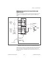
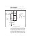
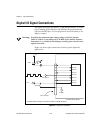
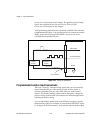
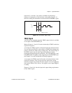
Figure 4-9 shows DIO<0, 2..3, 5..6> configured for digital input and
DIO<1, 4, 7> configured for digital output. Digital input applications
include receiving TTL signals and sensing external device states such
as the state of the switch. Digital output applications include sending
TTL signals and driving external devices such as the LED.
Power Connections
One pin on the I/O connector supplies +5 V from the VXIbus power
supply via a self-resetting fuse. The fuse will reset automatically after
you remove the overcurrent condition. These pins are referenced to
DGND and can be used to power external digital circuitry.
• Power rating +4.65 to +5.25 VDC at 1 A
Warning:
Under no circumstances should you connect these +5 V power pins directly
to analog or digital ground or to any other voltage source on the
VXI-MIO Series module or any other device. Doing so can damage the
VXI-MIO Series module and your device. National Instruments is
NOT
liable for damages resulting from such a connection.
Timing Connections
Warning:
Exceeding the maximum input voltage ratings, which are listed in
Tables 4-1 and 4-2, can damage the VXI-MIO Series module. National
Instruments is
NOT
liable for any damages resulting from incorrect signal
connections.
All external control over the VXI-MIO module timing is routed through
the 10 programmable function input signals labeled PFI<0..9>. These
signals are explained in detail in the
Programmable Function Input
Connections
section in this chapter. These PFI signals are bidirectional;
as output signals they are not programmable and reflect the state of
many data acquisition, waveform generation, and general-purpose
timing signals. There are five other dedicated output lines for the
remainder of the timing signals. As input signals, the PFI signals are
programmable and can control any data acquisition, waveform
generation, and general-purpose timing signals.
The data acquisition signals are explained in the
Data Acquisition
Timing Connections
section later in this chapter. The waveform
generation signals are explained in the
Waveform Generation Timing