


Hardware Reference
ARM DUI 0163B Copyright © 2001-2003. All rights reserved. 3-5
3.3 SPI
This interface module provides two connectors for SPI ports. They are connected
directly to the logic module FPGA and are used by the SSP PrimeCell (PL022) in the
example configuration.
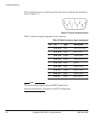
Table 3-3 shows the assignment of the SPI signals to the logic module signals on the
EXPIM connector.
Three chip select signals are provided to allow connection of three separate SPI devices.
The SPI signals are routed to two connectors, J11 and J13, for ease of connection to
different SPI devices, although both are connected to the same set of signals.
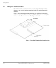
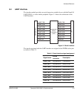
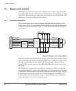
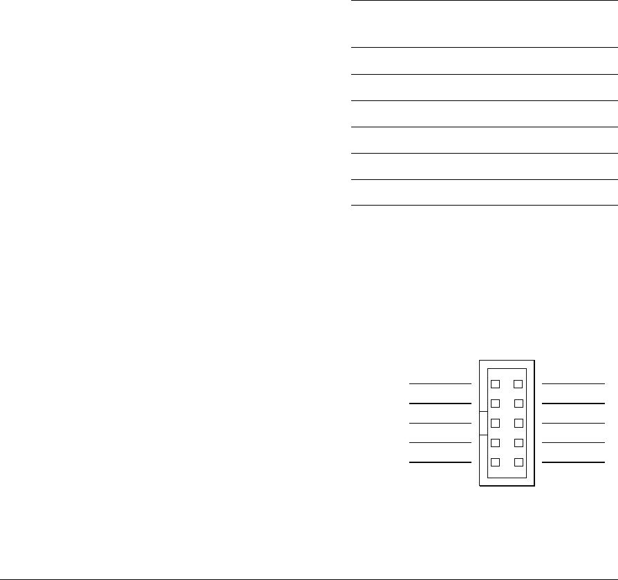
Figure 3-3 shows the pinout of the SPI connectors.
Figure 3-3 SPI interface connector pinout
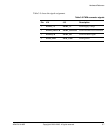
Table 3-3 SPI signals
Signal
EXPIM
connector
Description
SPI_CLK IM_BBANK31 SPI Clock
SPI_TXD IM_BBANK32 SPI transmit data
SPI_RXD IM_BBANK33 SPI receive data
SPI_nCS0 IM_BBANK34 SPI chip select 0
SPI_nCS1 IM_BBANK35 SPI chip select 1
SPI_nCS2 IM_BBANK36 SPI chip select 2
SPI_CLK
SPI_TXD
SPI_RXD
SPI_nCS0
SPI_nCS1
GND
+5V
+3V3
GND
SPI_nCS2
12
910
J11/J13