


Reference Design Example
4-10 Copyright © 2001-2003. All rights reserved. ARM DUI 0163B
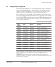
You must also observe the operating range limits:
Note
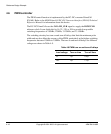
The default values for these registers set CLK1 to 25MHz and CLK2 to 12MHz.
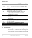
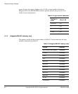
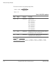
Table 4-5 LM_OSCx registers
Bits Name Access Function
18:16 OD Read/write Output divider:
000 = divide by 10
001 = divide by 2
010 = divide by 8
011 = divide by 4
100 = divide by 5
101 = divide by 7
110 = divide by 9
111 = divide by 6.
15:9 RDW Read/write Reference divider word. Defines the binary value of
the R[6:0] pins of the clock generator.
8:0 VDW Read/write VCO divider word. Defines the binary value of the
V[8:0] pins of the clock generator.
10MHz < 48MHz ·
(V[8:0] +8)
(R[6:0] +2)
R[6:0] < 118