


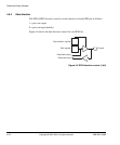

Reference Design Example
ARM DUI 0163B Copyright © 2001-2003. All rights reserved. 4-27
4.12 ADC and DAC interface
This interface gives you access to the ADCs and DAC. The interface also contains a
status and control register. The offset addresses of the ADC and DAC interface are
shown in Table 4-16.
The ADCs each appear as one 16-bit location at the corresponding base address. The
DAC appears as two locations at DACBase and DACBase+4 that correspond to the
DAC A and B channels respectively. Refer to the AD7859 and AD5342 data sheets for
details of ADC and DAC operations.
Accesses to these devices take four system bus clock cycles, although consecutive
accesses incur an additional three wait states for the second and subsequent access. The
DAC has the signal LDAC tied LOW. This means that a value is passed to the DAC as
soon as it is written.
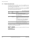
The ADC status register provides you with read-only access to the ADC busy signals.
The bit assignment is shown in Table 4-17.
The DACnCLR register provides you with read/write access to control the signal nCLR
routed to the DAC. Write 0 to this register to reset the DAC value to 0. You must write
a 1 to enable normal operation of the DAC.
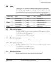
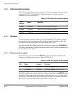
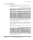
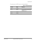
Table 4-16 ADC and DAC interface registers
Offset
address
Name Function
0x000000
ADCSTATUS This register enables you to monitor the status of the ADC
busy signals
0x000004
DACnCLR This register controls the nCLR signal to the DAC.
0x100000
ADC1Base Interface to ADC1
0x200000
ADC2Base Interface to ADC2
0x300000
DACBase Interface to the DAC
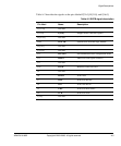
Table 4-17 ADC status register bit assignment
Bit Name Access Function
1 ADC2BUSY Read Gives value of ADC2 busy signal
0 ADC1BUSY Read Gives value of ADC1 busy signal