


Reference Design Example
ARM DUI 0163B Copyright © 2001-2003. All rights reserved. 4-21
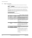
4.8 GPIO
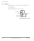
There are two 32-bit GPIO blocks instantiated in the example design. Each GPIO
provides 32 general-purpose input and output signals that are connected to the
connectors J16 and J17. GPIOB is also connected to the 38-way Mictor connector J7
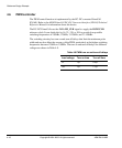
for easy connection to a logic analyzer. The GPIO registers are shown in Table 4-12.
4.8.1 Data output set register
The GPIO_DATASET location is used to set individual GPIO output bits as follows:
1 = SET the associated GPIO output bit
0 = leave the associated GPIO bit unchanged.
4.8.2 Read data input register
Read the current state of the GPIO input bits from this location.
4.8.3 Data register output clear
The GPIO_DATACLR location is used to clear individual GPIO output bits as follows:
1 = CLEAR the associated GPIO output bit
0 = leave the associated GPIO bit unchanged.
4.8.4 Read data output pins
Read the current state of the GPIO output bits from this location.
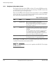
Table 4-12 GPIO registers
Address offset Name Access Size Function
0x000000
GPIO_DATASET Write 32 Data output set
GPIO_DATAIN Read 32 Read data input pins
0x000004
GPIO_DATACLR Write 32 Data register output clear
GPIO_DATAOUT Read 32 Read data output pins
0x000008
GPIO_DIRN Read/write 32 Data direction