


Hardware Reference
3-18 Copyright © 2001-2003. All rights reserved. ARM DUI 0163B
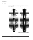
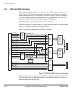
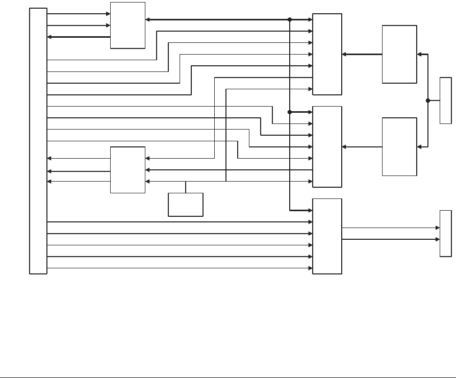
3.8 ADC and DAC interfaces
The interface module provides two A to D Converters (ADC) and a D to A Converter
(DAC). The two ADCs each provide eight analog inputs with buffered 0-5V inputs, an
internal multiplexer, and a 12-bit converter. The ADCs provide a 16-bit host interface
with conversion data appearing on D[11:0] (and zeros on D[15:12]). The ADCs are
clocked by a 4MHz crystal and are able to perform 200ksamples/s.
The DAC provides two 0-5V outputs with a 12-bit resolution.
The ADCs and DAC are powered from a 5V supply and share buffers to interface them
to the 3.3V system bus provided by the logic module.
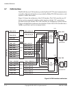
Figure 3-10 shows the architecture of the ADCs and DACs.
Figure 3-10 ADC and DAC interface architecture
All of the interface signals are routed to the FPGA on the logic module. The ADCs and
DAC are supported by an AHB interface that is instantiated in the logic module code
example supplied with the IM-AD1.
EXPIM socket
ADC
(U6)
ADC
(U10)
U13
AD_D[15:0]_5V
ADC1_nCS
ADC1_CONV
ADC1_RD
AD_D[15:0]
AD_T/R
AD_nOE
J1
Buffers
(U5
and
U8)
ADC1_nWR
ADC2_nCS
ADC2_CONV
ADC2_RD
ADC2_nWR
ADC2_BUSY
Buffer
(U7)
ADC1_BUSY
ADC_CLK
DAC
(U11)
XTAL
(U12)
ADC1_BUSY_5V
ADC_CLK_5V
DAC_nCLR
DAC_nLDAC
DAC_A0
DAC_nCS
DAC_nWR
J2
Buffers
(U1
and
U2
Buffers
(U3
and
U4)
AIN[7:0]
AIN[8:15]
ADC2_BUSY_5V