


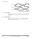
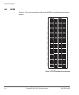
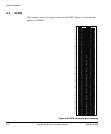

Reference Design Example
4-28 Copyright © 2001-2003. All rights reserved. ARM DUI 0163B
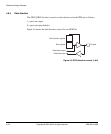
4.13 Peripheral information block
The Peripheral Information Block (PIB) is a block of 32 words in ROM that provides
you with information about the peripherals used in the design. The PIB is located at the
top of the address space for the logic module.
Each word in the PIB provides information about one peripheral. A value of
0x00000000
indicates that there is no entry and that the next address must be checked. Each valid
entry contains the information shown in Table 4-18.
The last address of the PIB is used to store the FPGA build number. Bits [31:8] are all
1 and bits [7:0] store the revision number in BCD.
Note
Use the ARM executable utility
read_pib.axf
, supplied on the IM-AD1 CD, to display
the PIB information.
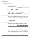
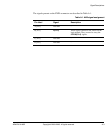
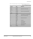
Table 4-18 PIB entry format
Bits Name Function
31:24 Peripheral Base Bits [27:20] of the peripheral base address.
Bits [31:28] of the address are defined by the location of
the logic module in the stack see Address assignment of
logic modules on page 4-5.
23:8 Peripheral ID For a PrimeCell, this is the PrimeCell number in BCD. For
example, the VIC PrimeCell PL190 would be represented
by
0x0190
.
For other peripherals the value
0xFFnn
is assigned, where
nn
is a unique look-up value. (See the AHBPIB HDL
source file for details.) The value
0xFFFF
is a special case
that is used to indicate the FPGA build number.
7:0 Peripheral Rev This gives the revision number of the peripheral in BCD.
For example, revision v1.2 is represented by
0x12
.