


Hardware Reference
3-20 Copyright © 2001-2003. All rights reserved. ARM DUI 0163B
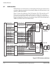
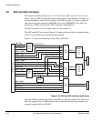
The analog inputs to the ADCs are buffered by LMV324 operational amplifiers
(op-amps). The op-amps are configured to give unity gain but the inputs have a resistive
divider that divides the input voltage by 2. A 0-5V input signal range at the buffer inputs
provides a 0-2.5V full range at the ADC input. If different input ranges are required the
divider resistor values can be changed.
The op-amp buffers cannot drive their outputs lower than 65mV. This means input
signals less than 130mV will have incorrect ADC values.
The reference voltage from one of the ADCs is buffered and fed to the reference inputs
of the other ADC and the DAC so that all devices share a common reference. The GAIN
input to the DAC is tied HIGH to configure the output range of the DAC to be 0 to
2xVref.
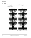
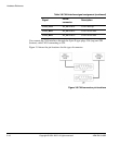
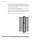
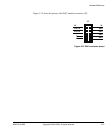
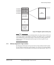
Figure 3-11 shows the pinout of the ADC interface connector (J1).
Figure 3-11 ADC connector pinout
ADC0
ADC1
ADC2
ADC3
ADC4
ADC5
ADC6
ADC7
ADC8
ADC9
GND
GND
GND
GND
GND
GND
GND
GND
GND
GND
1
33
2
34
ADC10
ADC11
ADC12
ADC13
ADC14
ADC15
GND
GND
GND
5V 5V
GND
GND
GND
J1