Hardware Configuration 2-3
NOTE: The Base I/O address and IRQ settings are the
same for all adapters. Data Clock Direction, DTE,
is correct for all connections except V.35.
Other switch or jumper settings unique to an individual adapter type (i.e.,
DCP286i-SBC, DCP386i, or DCP486e) are detailed in a separate section of
this chapter specific to each adapter.
Base I/O Address
The Base I/O address is selected via switch SW1, which may be labeled CR
ADDR (Control Register Address) on some adapters.
The adapter requires four bytes of I/O locations for its control registers.
These control registers are used by the server CPU to coordinate and service
information provided by the adapter. The address of these registers depends
on the setting of switches SW1-1 through SW1-4. The factory default is set
to 33C hex.
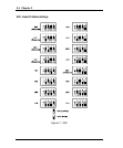
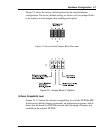
Figure 2-1 shows the possible settings for the Control Register 1 address. To
locate the position of SW1 on the adapter, refer to the appropriate diagram in
the following sections for the adapter type you are installing (i.e. 286, 386 or
486).


