


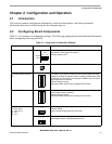

Configuration and Operation
M9328MX21ADSE User’s Manual, Rev. A
Freescale Semiconductor 2-1
Chapter 2 Configuration and Operation
2.1 Introduction
This section contains configuration information, connection descriptions, and other operational
information that may be useful during the development process.
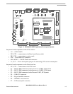
2.2 Configuring Board Components
Table 2-1 is a summary of configuration settings. The following paragraphs provide additional information
about configuring and using the ADS.
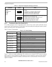
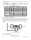
Table 2-1. Component Configuration Settings
Component Position Effect
System Power Switch, SW1 Move this switch to the ON position to enable the power source
connected to P8 to power the system.
Factory setting is OFF.
System Reset Switch, SW2 Push to reset the M9328MX21ADSE.
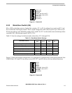
Peripheral Selection Switch,
S1
S1
The UART1 and UART4 transceivers are forced enabled, the IrDA
module is enabled by software, Nexus is disabled, ARM mode JTAG
is selected, and the buzzer is connected to PWMO. The LCD touch
panel signals are connected.
Factory setting is shown.
Subsection 2.2.1 explains other settings for this switch.
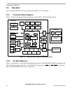
Mode Switch, S2
S2
Configures 32-bit Burst Flash as the boot device and the Default
clock bypass mode is selected.
Factory setting is shown
Subsection 2.2.2 explains other settings for this switch.
Power Headers
(on CPU card)
J1, VCC (3.0 V)
J2, 1.8 V
J3, 1.5 V
Connects specified power signal.
Factory Setting
(Leave jumper installed during normal use.)
Connect ammeter across pins to measure processor current
consumption from the specified power source.
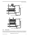
SW1
ON
OFF
BOARD
EDGE
SW2
5
ON
4
8
S1
1
2
3
6
7
5
ON
4
8
S2
1
2
3
6
7
12
12