


Support Information
M9328MX21ADSE User’s Manual, Rev. A
3-10 Freescale Semiconductor
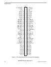
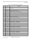
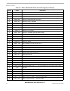
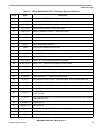
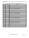
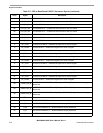
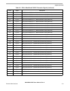
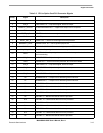
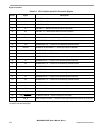
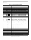
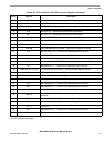
62 CPU_BD_ID0 CPU BOARD ID 0 — Indicates the build revision of the CPU board
63 CPU_BD_ID7 CPU BOARD ID 1 — Indicates the build revision of the CPU board
64 CPU_BD_ID1 CPU BOARD ID 2 — Indicates the build revision of the CPU board
65 CPU_BD_ID6 CPU BOARD ID 3 — Indicates the build revision of the CPU board
66 CPU_BD_ID2 CPU BOARD ID 4 — Indicates the build revision of the CPU board
67 CPU_BD_ID5 CPU BOARD ID 5 — Indicates the build revision of the CPU board
68 CPU_BD_ID3 CPU BOARD ID 6 — Indicates the build revision of the CPU board
69 CPU_BD_ID4 CPU BOARD ID 7 — Indicates the build revision of the CPU board
71 KP_COL5 KEYPAD COLUMN 5 — Bidirectional signal use to scan a keypad
72 KP_ROW5 KEYPAD ROW 5 — Bidirectional signal use to scan a keypad
73 KP_COL4 KEYPAD COLUMN 4 — Bidirectional signal use to scan a keypad
74 KP_ROW4 KEYPAD ROW 4 — Bidirectional signal use to scan a keypad
75 KP_COL3 KEYPAD COLUMN 3 — Bidirectional signal use to scan a keypad
76 KP_ROW3 KEYPAD ROW 3 — Bidirectional signal use to scan a keypad
77 KP_COL2 KEYPAD COLUMN 2 — Bidirectional signal use to scan a keypad
78 KP_ROW2 KEYPAD ROW 2 — Bidirectional signal use to scan a keypad
79 KP_COL1 KEYPAD COLUMN 1 — Bidirectional signal use to scan a keypad
80 KP_ROW1 KEYPAD ROW 1 — Bidirectional signal use to scan a keypad
81 KP_COL0 KEYPAD COLUMN 0 — Bidirectional signal use to scan a keypad
82 KP_ROW0 KEYPAD ROW 0 — Bidirectional signal use to scan a keypad
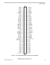
83 B_DQM0_EB0_B
BUFFERED ENABLE BYTE 0 — D[31:24] for SDRAM, [D7:0] for other memory types
(Reserved)
84 B_DQM1_EB1_B
BUFFERED ENABLE BYTE 1 — D[23:16] for SDRAM, D[15:8] for other memory types
(Reserved)
85 B_DQM2_EB2_B
BUFFERED ENABLE BYTE 2 — D[15:8] for SDRAM, D[23:16] for other memory types
(Reserved)
86 TP21 Test point
87 B_A4 BUFFERED ADDRESS 4 — Buffered address output (Reserved)
88 B_A5 BUFFERED ADDRESS 5 — Buffered address output (Reserved)
89 B_A6 BUFFERED ADDRESS 6 — Buffered address output (Reserved)
90 B_A7 BUFFERED ADDRESS 7 — Buffered address output (Reserved)
91 B_A8 BUFFERED ADDRESS 8 — Buffered address output (Reserved)
Table 3-2. CPU to Base Board PX2/PY2 Connector Signals (continued)
Pin(s) Signal Description