


General Information
M9328MX21ADSE User’s Manual, Rev. A
Freescale Semiconductor 1-3
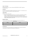
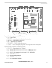
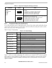
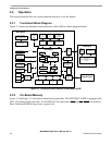
Figure 1-1. M9328MX21ADSE Application Development System
Important board components on the CPU card are:
• U5 — i.MX21 MCU
• PX1, PX2 — connections to the Base board (bottom side)
• PK1, PK2 — connections to option cards
• P20 — ARM Multi-ICE connector
• PM1 & PM2 — NAND Flash card connectors
• J1, J2, J3 — Power interruption jumpers for measuring CPU current consumption
Important board components on the Base board are:
• PY1, PY2 — connections to the CPU board
• P1 — RS-232 DB9 connector for the processor’s UART1, DCE pinout
• P2 — RS-232 DB9 connector for the processor’s UART4, DTE pinout
• P3 — RS-232 DB9 connector for the External UART, DCE pinout
• P4 — USB OTG connector
• P5 — Keypad module connector
• P6 — SD/MMC card connector
• P7 — LCD/touch panel connector
TV ENCODER
CON
LCD CON
+5V IN
P8
F1
SW1
P9
P3 P2 P1
P4
U16
VR1
P7
P5
KEYPAD CON
P6
PE1
CSI
PE2PE3
EXP CON 2
EXP CON 1
J7
ONE WIRE
P10
P11
P12
S1
LED2
LED3
LED4
LED7
LED6 LED5
LINE IN
MIC IN
HEADPHONE
P20
PK1
PK2
J3J1 J2
CPU BOARDBASE BOARD
ON
OFF
2A
ETHERNET
EXT UART DCE UART4 DTE UART1 DCE USB OTG
BATT EM
IrDA
ACT
SD2_D0
P13
SD/MMC
UART1_ON
UART4_ON
IrDA_ON
NEXUS_EN
JTAG_CTRL
TONE_OUT
PEN_CS_B
PEN_IRQ_B
LED1
1
2
3
4
5
6
7
8
S2
BOOT0
BOOT1
BOOT2
BOOT3
CLKMODE0
CLKMODE1
SW1 IRQ
SW2 READ
1
2
3
4
5
6
7
8
LINK ACT
RESET
SW2
BUZZER
VCC PWR
STAT2
STAT1
BUS ACT
5V PWR
DTR
J3
NC
SD2_D1
DSR
J4
NC
SD2_D2
CD
J5
SD2_D3
NC
RI
J6
MULTI-ICE
U5
CPU
PX1/PY1
PX2/PY2
U6
U8
U7
U9
3
2
1
PM1
PM2
NAND FLASH CARD