


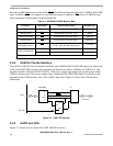

Configuration and Operation
M9328MX21ADSE User’s Manual, Rev. A
2-10 Freescale Semiconductor
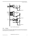
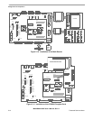
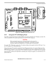
2.3.10 Memory Mapped I/O
The ADS uses Memory Mapped I/O to add I/O functions without using the I/O resources of the processor.
The following paragraphs describe the I/O functions.
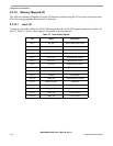
2.3.10.1 Input I/O
A memory read of hex address 0xCC80_0000 inputs the state of the ADS signals connected to latches U5
and U7. Table 2-7 shows which signal is associated with each data bit.
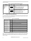
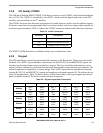
Table 2-7. Input Buffer Signals
BIT Signal Description
BIT 0 SD_WP Secure Data Write Protect
BIT 1 SW_SEL Software readable switch
BIT 2 RESET_E_UART External UART Reset
BIT 3 RESET_BASE Ethernet controller Reset
BIT 4 CSI_CTL2 Image Sensor control 2
BIT 5 CSI_CTL1 Image Sensor control 1
BIT 6 CSI_CTL0 Image Sensor control 0
BIT 7 UART1_EN UART1 transceiver enable
BIT 8 UART4_EN UART4 transceiver enable
BIT 9 LCDON LCD enable
BIT 10 IRDA_EN IrDA transceiver enable
BIT 11 IRDA_FIR_SEL Reserved
BIT 12 IRDA_MD0_B IrDA SD/Mode (inverted)
BIT 13 IRDA_MD1 Reserved
BIT 14 LED4_ON LED 4 control
BIT 15 LED3_ON LED 3 control