


Support Information
M9328MX21ADSE User’s Manual, Rev. A
Freescale Semiconductor 3-13
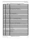
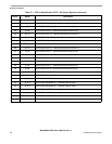
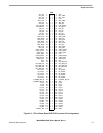
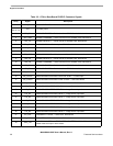
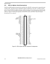
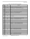
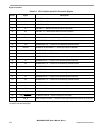
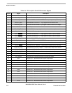
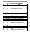
Table 3-3. CPU to Option Card PK1 Connector Signals
Pin(s) Signal Description
1, 45 VCC +3.0 VDC power
2 CS0_B CHIP SELECT 0 — Chip select signal, active low output
3PWMO PC_SPKOUT PCMCIA SPEAKER OUT — Digital audio output to drive a speaker*
4 TP13 Test point
5 RESET_IN_B RESET IN — Active low reset signal to the processor
6, 9 P2.5V +2.5 VDC power
7 RESET_OUT_B RESET OUT — Active low reset signal from the processor
8 NEXUSEVTI_GPIO NEXUS EVENT IN — can be general purpose I/O
10 SDCKE1 SDRAM CLOCK ENABLE 1 — Active high outputs to SDRAM
11 RW_B PC_WE PCMCIA — Output signal used to latch memory write data*
12 BCLK
BURST CLOCK — Output signal to external burst devices; synchronizes burst loading
and incrementing
13 CS5_B CHIP SELECT 5 — Chip select signal, active low output
14 CLKO CLOCK OUT — Clock out from the processor, NC if R44 not installed
15 CS3_B CHIP SELECT 3 — Chip select signal, active low output
16 CS4_B CHIP SELECT 4 — Chip select signal, active low output
17, 51 P1.8v +1.8 VDC power
18 CS1_B CHIP SELECT 1 — Chip select signal, active low output
19 A0 ADDRESS BIT 0 — Output line for addressing external devices.
20 A1 ADDRESS BIT 1 — Output line for addressing external devices.
21 D7 DATA BIT 7 — Bidirectional data bit from the processor
22 D8 DATA BIT 8 — Bidirectional data bit from the processor
23 D6 DATA BIT 6 — Bidirectional data bit from the processor
24 D9 DATA BIT 9 — Bidirectional data bit from the processor
25 D5 DATA BIT 5 — Bidirectional data bit from the processor
26 D10 DATA BIT 10 — Bidirectional data bit from the processor
27 D4 DATA BIT 4 — Bidirectional data bit from the processor
28 D11 DATA BIT 11 — Bidirectional data bit from the processor
29 D3 DATA BIT 3 — Bidirectional data bit from the processor
30 D12 DATA BIT 12 — Bidirectional data bit from the processor
31 D2 DATA BIT 2 — Bidirectional data bit from the processor