


M9328MX21ADSE User’s Manual, Rev. A
Freescale Semiconductor 3-1
Chapter 3 Support Information
3.1 Introduction
This section contains connector pin assignments, connector signal descriptions, and other useful
information about the M9328MX21ADSE. Both the CPU and Base board connectors are described.
The tables in this section list signal names as they appear in the schematics for the boards. The figures
usually refer to the same signal name, but may substitute a generally accepted standard name for that
function. For example, all RS-232 transmitted data signals are referred to as TXD regardless of which
RS-232 connector is being illustrated. Also, the use of “_B” at the end of a signal name indicates that the
active state of the signal is logic level zero or ground potential (active low).
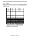
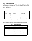
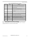
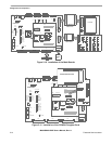
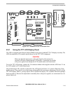
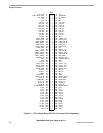
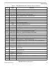
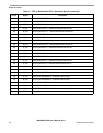
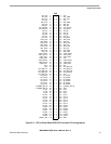
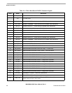
3.2 CPU to Base Board Connectors PX1, PX2, PY1, and PY2
The PX1 and PX2 connectors located at the bottom side of the ADS CPU card connect this board to the
ADS Base board through connectors PY1 and PY2 located on the top side of the board. Figure 3-1 shows
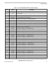
the pin assignments for the PX1 and PY1 connectors. Table 3-1 provides signal descriptions for these
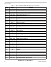
connectors. Figure 3-2 shows the pin assignments for the PX2 and PY2 connectors and Table 3-2 provides
signal descriptions for these connectors.