


Support Information
M9328MX21ADSE User’s Manual, Rev. A
Freescale Semiconductor 3-27
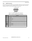
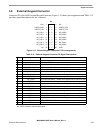
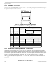
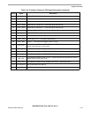
3.11 TV Encoder Connector
Connector P13 is the TV encoder connector. Figure 3-15 gives the pin assignments and Table 3-15 gives
the signal descriptions for this connector.
Figure 3-15. TV encoder Connector P13 Pin Assignments
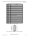
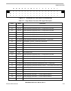
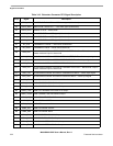
18 LD14_R2 LCD DATA 14 / RED BIT 2 — Output data to LCD
19 CONTRAST LCD bias voltage used as contrast control
20 LCDON LCD enable — Active High, Enables the Sharp LCD
21 SPL_SPR SAMPLING LEFT to RIGHT— Horizontal scan direction
22 REV Signal for common electrode driving signal preparation (Sharp panel dedicated signal)
23 PS Control signal output for source driver (Sharp panel dedicated signal)
24 CLS
Start signal output for gate driver. This signal is inverted version of PS (Sharp panel
dedicated signal)
25 LD1_B1 LCD DATA 1 / BLUE BIT 1 — Output data to LCD
26 LD0_B0 LCD DATA 0 / BLUE BIT 0 — Output data to LCD
27 LD7_G1 LCD DATA 7 / GREEN BIT 1 — Output data to LCD
28 LD6_G0 LCD DATA 6 / GREEN BIT 0 — Output data to LCD
29 LD13_R1 LCD DATA 13 / RED BIT 1 — Output data to LCD
30 LD12_R0 LCD DATA 12 / RED BIT 0 — Output data to LCD
31 TOP Negative pen-Y analog input
32 BOTTOM Positive pen-Y analog input
33 LEFT Negative pen-X analog input
34 RIGHT Positive pen-X analog input
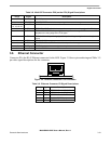
P13
VCC 1 • • 2P5V
I2C_CLK 3 • • 4NC
I2C_DATA 5 • • 6NC
GND 7 • • 8GND
CLK_26M 9 • • 10 GND
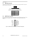
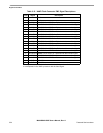
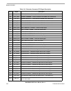
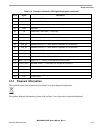
Table 3-15. TV encoder Connector P13 Signal Descriptions
Pin(s) Signal Description
1 VCC +3 VDC power
2 P5V +5 VDC power
3 I2C_CLK I SQUARED C CLOCK — Serial clock, bidirectional
4,6 NC NO CONNECTION
5 I2C_DATA I SQUARED C DATA — Serial data, bidirectional
7, 8, 10 GND GROUND
9 CLK_26M 26M Clock signal from TV encoder card
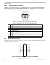
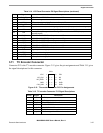
Table 3-14. LCD Panel Connector P8 Signal Descriptions (continued)
Pin(s) Signal Description