


Configuration and Operation
M9328MX21ADSE User’s Manual, Rev. A
2-4 Freescale Semiconductor
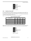
2.3 Operation
This section describes how the system functions and how to use the boards.
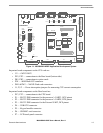
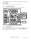
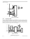
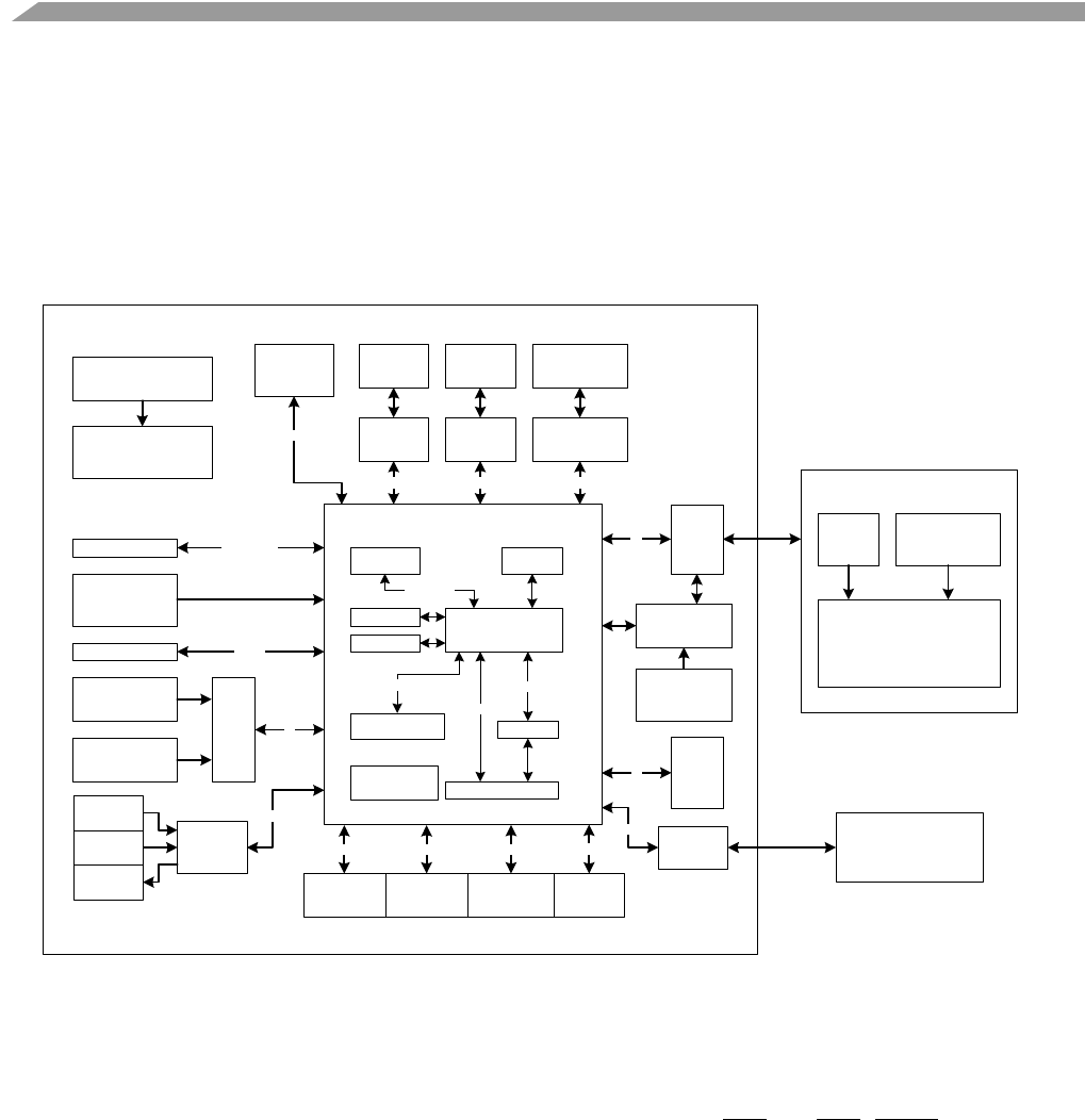
2.3.1 Functional Block Diagram
Figure 2-3 shows the functional interconnections of the ADS in a block diagram format.
Figure 2-3. Functional Block Diagram of M9328MX21ADSE
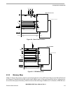
2.3.2 On-Board Memory
Figure 2-4 and Figure 2-5 show the on-board memory interface. The M9328MX21ADSE is equipped with
8M x 32-bit Burst Flash and 16M x 32-bit SDRAM. The chip selects CS0
and CS2 (CSD0) are used for
Burst Flash and SDRAM chip selects, respectively.
i.MX21
SDRAM
Burst Flash
Transceiver
CPU Board
High Speed
Connectors
Base board connectors
Addr /Data bus
Addr /Data bus
IO pins
Ethernet
port
USB series
mini-AB
connector
UART1,
UART2 &
IrDA
Ext.
UART
LEDs & Buzzer
Boot mode,
UARTs, IrDA
selection
1-wire Interface
Silicon & Board
revision register
S/W readable
DIP switches
Audio
CODEC
UART
controller
Ethernet
controller
USB OTG
Transceiver
IO pins , PWM
OWIRE
Peripheral signals CSI signals MMC/SD signals
LCDC
USBOTG signalsAddr /Data BusAddr /Data Bus
UART signals
Decoder & Chip
select logic
Addr/Data Bus
SSI
Base Board
Power Connector,
Power Switch & fuse
3V regulator, CPU
Reset signal
LCD
connector
Battery Level
Measurement
Emulation
Touch screen
controller
LCD panel
(240x320 pixels) & Touch
screen
White
LED
driver
LCD Board
TFT LCD DC-
DC converter
Keypad
Connector
Keypad Board
KPP
NAND Flash
Connector
Multi-ICE
connector
NFC signals
TV
Encoder
connector
I2C
Line In
Speaker
Out
Mic In
MMC/SD
connector
Image sensor
connector
Expansion
Connector 1
Expansion
Connector 2
Peripheral signals
2.5V, 1.8V and
1.5V regulators