


Contents-4
HP 8517B S-Parameter Test Set Manual
UnratioedPowerTest ................................ 5-14
Figure 5-9. Diagram of IF Signal Path ..................... 5-14
IsolatingSignalPathProblems ............................ 5-14
TestingSignalPaths1-4.............................. 5-14
TestingPaths5and6 ................................ 5-16
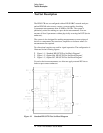
Figure 5-10. RF Path 1 and Path 2, HP 8517B Standard Test Set .5-17
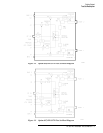
Figure 5-11. RF Path 3 and Path 4, HP 8517B Standard Test Set .5-18
Figure 5-12. RF Path 5 and Path 6, HP 8517B Standard Test Set .5-19
Figure 5-13. RF Path 1 through Path 4,
HP 8517B Option 007 Test Set ......................... 5-20
Figure 5-14. RF Signal for Path 1 through Path 4,
HP 8517B Option 007 ............................... 5-21
Figure 5-15. RF Path 5 and Path 6, HP 8517B Option 007 ...... 5-22
Table 5-6. Test Results for Path 1 through Path 6 ............. 5-23
SampleDiagnostics..................................... 5-23
Table 5-7. Most Probable Failures
(B indicates Bad; — indicates Good) .................... 5-23
6. HP 8517B Test Set Replacement Procedures
Figure 6-1. ESD-Safe Workstation Configuration .............. 6-2
PerformanceTests .......................................... 6-2
Adjustments ............................................... 6-2
Equipment Needed But Not Supplied . .......................... 6-3
Table 6-1. Replacement-Procedure Tools Needed .............. 6-3
Figure 6-2. HP 8517B Major Assembly Location Diagram ...... 6-4
AssemblyReplacementProcedures............................. 6-5
InitialPrecautions ....................................... 6-5
Switch/SplitterReplacement............................... 6-5
A18Switch/SplitterAssembly .......................... 6-5
FrequencyConverterReplacement .......................... 6-5
A14,A10toA13FrequencyConverterAssembly .......... 6-5
RegulatorBoardReplacement ............................. 6-6
A15RegulatorBoardAssembly......................... 6-6
FilterCapacitorReplacement .............................. 6-6
C1toC4FilterCapacitors ............................. 6-6
TestPortConnectorReplacement........................... 6-7
2.4mmTestPortConnectors ........................... 6-7
Figure 6-3. Diagram of 2.4 mm Test Port Connector ............ 6-7
FanAssemblyReplacement ............................... 6-8
B1FanAssembly .................................... 6-8
PowerTransformerReplacement ........................... 6-8
T1PowerTransformer ................................ 6-8
Figure 6-4. Wire Connections to FL1 Line Module ............. 6-9
O-RingReplacement.................................... 6-10
Figure 6-5. Positioning the O-Ring Within the Clamp .......... 6-10
FrontPanelandInterfaceBoardReplacement ................ 6-10
A1FrontPanelandInterfaceBoardAssembly ............ 6-10