


EM78P312N
8-Bit Microcontroller
Product Specification (V1.0) 10.03.2006
• 17
(This specification is subject to change without further notice)
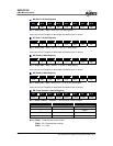
In using the external clock, data input sample is fixed at the middle of data output time.
Bit 6 ( DCOL ) : SPI Data collision.
DCOL = “0” : No occurrence of Data collision
DCOL = “1” : Data collision occurred. It should be cleared by software.
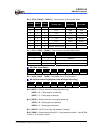
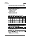
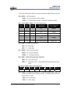
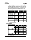
Bit 5 ~ Bit 3 ( BRS0 ~ BRS2 ) : SPI Clock Source Select
BRS2 BRS1 BRS0
Clock Source
( Normal, Idle )
Max. Transfer Rate
( Fc = 8MHz )
0 0 0 Fc/2
13
0.95Kbit/s
0 0 1 Fc/2
11
3.8Kbit/s
0 1 0 Fc/2
10
7.6Kbit/s
0 1 1 Fc/2
8
30.5Kbit/s
1 0 0 Fc/2
6
122Kbit/s
1 0 1 Fc/2
5
244Kbit/s
1 1 0 External clock (/SCK pin) Enable /ss pin
1 1 1 External clock (/SCK pin) Disable /ss pin
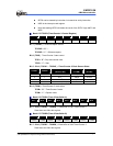
Bit 2 ( EDS ) : Data shift out edge select.
EDS = “0” : Rising edge
EDS = “1” : Falling edge
Bit 1 ( DORD ) : Data transmission order.
DORD = “0” : Shift left (MSB first)
DORD = “1” : Shift right (LSB first)
Bit 0 ( WBE ) : Write buffer empty flag. Read only.
WBE = “0” : Write buffer empty
WBE = “1” : Not empty, set to “1” automatically when writing data to the data
buffer.
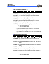
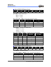
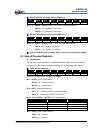
Bank 3 R6 SPIC2 (SPI Control Register 2)
Bit 7 Bit 6 Bit 5 Bit 4 Bit 3 Bit 2 Bit 1 Bit 0
SPIS 0 0 0 0 SPIM1 SPIM0 RBF
Bit 7 ( SPIS ) : SPI start shift, set the bit to “1” and shift register starts to shift. It is
cleared by hardware when shifting is finished. In transferring the next data, it
must be set to “1” again.
SPIS = “0” : Finish shifting
SPIS = “1” : Start shifting