


EM78P312N
8-Bit Microcontroller
32 •
Product Specification (V1.0) 10.03.2006
(This specification is subject to change without further notice)
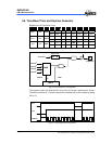
5.8.1 Serial Clock
Six internal clocks can be selected by setting BRS0 ~ BRS2 and the clock output to the
outside from /SCK (P70) pin. The External clock can also be used and connected to
/SCK (P70) pin.
5.8.2 Shift Direction and Sample Phase
Setting up the DORD bit of the SPIC1 register can determine the shift direction. Setting
up the EDS bit of the SPIC1 register can select the rising edge or falling edge and latch
the data. Setting up the SMP bit of the SPIC2 register can select the sample phase at
the middle or at the end of the data output time.
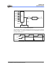
5.8.3 Transfer Mode
The transmit, receive, transmit/receive mode can be selected by setting SPIM0 ~
SPIM1.
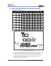
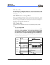
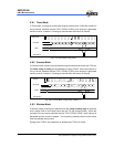
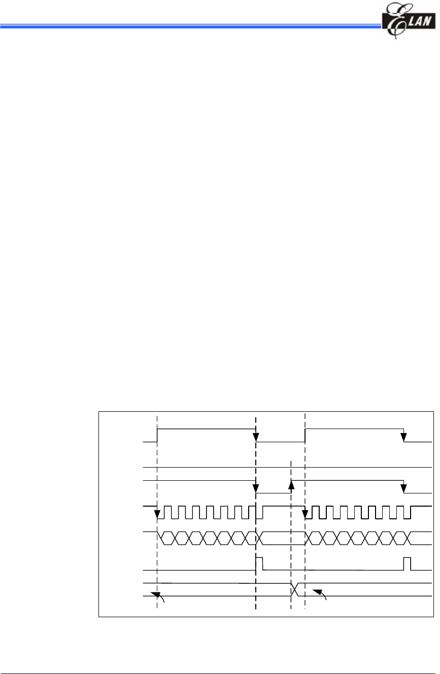
(a) 8-bit Transmit Mode
Set SPIM0 ~ SPIM12 to transmit mode and write data to the data buffer SPID.
Set SPIS to “1” to start transmission. The data are output sequentially to the SO
pin in synchronous with the serial clock. When the final bit of transfer data has
been transferred, the SPI interrupt is generated and SPIS is cleared to “0” by
hardware. In order to transmit the next data, the SPIS must be set to “1” again by
software. If the next data is not written to the data buffer, the transfer is not
started when using the internal clock.
SPI S
RBF
WBE
SPI F
shi f t f i ni sh
write data
shi f t start shi f t start
SO pi n
a0 a1 a2 a3 a4 a5 a6 a7
ab
SPI D
b0 b1 b2 b3 b4 b5 b6 b7
write data
Fig. 5-14 Transmit Mode (8-bit, 1 word)