EM78P312N
8-Bit Microcontroller
22 •
Product Specification (V1.0) 10.03.2006
(This specification is subject to change without further notice)
Bit 1 ( SPIE ) : SPI Interrupt enable bit.
SPIE = “0” : disable SPIF interrupt
SPIE = “1” : enable SPIF interrupt
Bit 0 ( TCIE3 ) : Timer/Counter 3 Interrupt enable bit.
TCIE3 = “0” : disable TCIF3 interrupt
TCIE3 = “1” : enable TCIF3 interrupt
Individual interrupt is enabled by setting its associated control bit in the IMR1 to "1".
Global interrupt is enabled by the ENI instruction and is disabled by the DISI instruction.
The IMR1 register is both readable and writable.
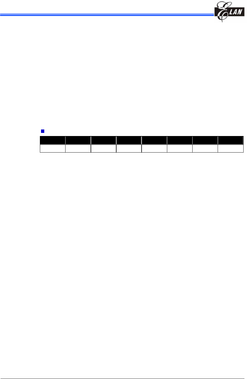
IMR2 − Interrupt Mask Register 2( Address: 0Fh )
Bit 7 Bit 6 Bit 5 Bit 4 Bit 3 Bit 2 Bit 1 Bit 0
0 UERRIE URIE UTIE TBIE EXIE1 0 TCIE0
Bit 6 ( UERRIE ) : UART receive error interrupt enable bit.
UERRIE = “0” : disable UERRIF interrupt
UERRIE = “1” : enable UERRIF interrupt
Bit 5 ( URIE ) : UART receive mode interrupt enable bit.
URIE = “0” : disable RBFF interrupt
URIE = “1” : enable RBFF interrupt
Bit 4 ( UTIE ) : UART transmit mode interrupt enable bit.
UTIE = “0” : disable TBEF interrupt
UTIE = “1” : enable TBEF interrupt
Bit 3 ( TBIE ) : Time base timer interrupt enable bit.
TBIE = “0” : disable TBIF interrupt
TBIE = “1” : enable TBIF interrupt
Bit 2 ( EXIE1 ) : External INT 1 Interrupt enable bit.
EXIE1 = “0” : disable EXIF1 interrupt
EXIE1 = “1” : enable EXIF1 interrupt
Bit 0 ( TCIE0 ) : TCC Interrupt enable bit.
TCIE0 = “0” : disable TCIF0 interrupt
TCIE0 = “1” : enable TCIF0 interrupt
Individual interrupt is enabled by setting its associated control bit in the IMR2 to "1".
Global interrupt is enabled by the ENI instruction and is disabled by the DISI instruction.
The IMR2 register is both readable and writable.


