


EM78P312N
8-Bit Microcontroller
42 •
Product Specification (V1.0) 10.03.2006
(This specification is subject to change without further notice)
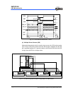
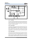
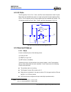
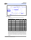
5.13 I/O Ports
The I/O registers, Port 6, Port 7, Port 8, and Port 9 are bi-directional tri-state I/O ports.
Each I/O pin can be defined as “input” or “output” pin by the I/O control register (IOC6 ~
IOC9). The I/O registers and I/O control registers are both readable and writable. The
I/O interface circuits for Port 6, Port 7, Port 8, and Port 9 are shown in Fig. 5-26.
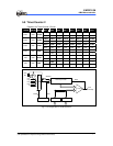
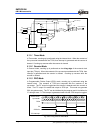
PDRD
Q
Q
CLK
D
P
R
C
L
PCWR
PDWR
Q
Q
CLK
D
P
R
C
L
PORT
0
1
M
U
X
IOD
PCRD
Fig. 5-27 The I/O Port and I/O Control Register Circuit
5.14 Reset and Wake-up
5.14.1 Reset
A reset is initiated by one of the following events:
(1) Power-on reset
(2) /RESET pin input “low”
(3) WDT timeout. (if enabled)
The device is kept in a reset condition for a period of approx. 18ms
1
(one oscillator
start-up timer period) after the reset is detected. Once a reset occurs, the following
functions are performed.
The oscillator starts or is running
The Program Counter (R2) is reset to all “0”.
When power is switched on, the upper two bits of R3, the upper two bits of R4 and
the Bits 6 ~ 4 of R5 are cleared.
All I/O port pins are configured as input mode (high-impedance state).
1
Note: VDD = 5V, set up time period = 16.2ms ± 30%
V
DD = 3V, set up time period = 19.6ms ± 30%