


EM78P312N
8-Bit Microcontroller
Product Specification (V1.0) 10.03.2006
• 5
(This specification is subject to change without further notice)
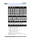
R0 (Indirect Addressing Register)
R0 is not a physically implemented register. Its major function is to act as an indirect
addressing pointer. Any instruction using R0 as a pointer actually accesses data
pointed by the RAM Select Register (R4).
R1 (Time Clock /Counter)
This register is writable and readable just like the other registers. The contents of the
prescaler counter are cleared only when a value is written into the TCC register.
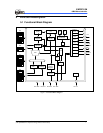
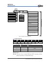
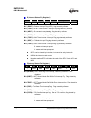
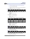
R2 (Program Counter) & Stack
z Depending on the device type, R2 and hardware stack are 10-bit wide. The
structure is depicted in Fig.5-3.
z Generates 8192 ×13 bits on-chip OTP ROM addresses to the relative
programming instruction codes. One program page is 1024 words long.
z R2 is set as all "0"s when under RESET condition
z "JMP" instruction allows direct loading of the lower 10 program counter bits.
Thus, "JMP" allows the PC to go to any location within a page.
z "CALL" instruction loads the lower 10 bits of the PC, and then PC+1 is pushed
onto the stack. Thus, the subroutine entry address can be located
anywhere within a page.
z "RET" ("RETL k", "RETI") instruction loads the program counter with the
contents of the top-level stack.
z All instructions are single instruction cycle (fclk/2 or fclk/4) except for the
instruction that would change the contents of R2. Such instruction will need
one more instruction cycle.
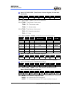
z For an interrupt trigger, the program ROM will jump to individual interrupt
vector at Page 0. The CPU will store ACC, R3 status and R5 PAGE
automatically, it will restore after instruction RETI.