


EM78P312N
8-Bit Microcontroller
24 •
Product Specification (V1.0) 10.03.2006
(This specification is subject to change without further notice)
In Sleep mode, the internal oscillator is turned off and all system operation is halted. Sleep
mode is released by /SLEEP pin (level sensitive or edge sensitive can be set by System
Control Register (SCR) Bit 0 (REM)). After a warm-up period, the next instruction will be
executed which is after the Sleep mode start instruction. Sleep mode can also be released
by setting the /RESET pin to low and executing a reset operation. In level sensitive mode,
the /SLEEP pin must be confirmed in low level before entering Sleep mode. In edge
sensitive mode, Sleep mode is started even when the /SLEEP pin is in high level.
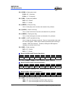
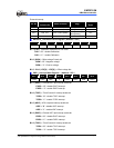
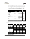
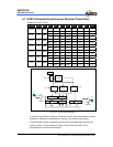
Table 4. Wake-up Methods
Wake-up Signal
Sleep Mode
R5 (SIS) = 1+SLEP
Instruction
Idle Mode
R5 (SIS)= 0 + SLEP
Instruction
Normal Mode
R5 (SIS)=(*)
1. Individual interrupt source
in IMR1, IMR2
2. WDT interrupt request
3. /INT0
4. ENI instruction is not
executed
No effect **
1. Wake-up
2. Jump to the next
instruction or enter
Idle mode
No effect
**
1. Individual interrupt source
in IMR1, IMR2
2. WDT interrupt request
3. /INT0
4. Execute ENI instruction
No effect **
1. Wake-up
2. Jump to an Interrupt
vector after RETI
instruction, then jump
to the next instruction
or enter Idle mode
Interrupt
/SLEEP pin
1. Wake-up
2. Jump to the next
instruction or enter
Sleep mode
No effect No effect
/RESET pin Reset Reset Reset
WDT time out Reset Reset Reset
Note: * Don’t care
** Interrupt request flag will be recorded
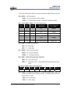
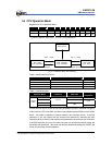
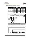
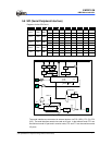
5.5 AD Converter
Registers for AD Converter Circuit
R_BANK Address NAME Bit 7 Bit 6 Bit 5 Bit 4 Bit 3 Bit 2 Bit 1 Bit 0
ADREF ADRUN ADCK1 ADCK0 ADP ADIS2 ADIS1 ADIS0
Bank 1 0X0B ADCR
R/W R/W R/W R/W R/W R/W R/W R/W
ADE7 ADE6 ADE5 ADE4 ADE3 ADE2 ADE1 ADE0
Bank 1 0X0C ADIC
R/W R/W R/W R/W R/W R/W R/W R/W
ADD9 ADD8 ADD7 ADD6 ADD5 ADD4 ADD3 ADD2
Bank 1 0X0D ADDH
R R R R R R R R
ADD1 ADD0 0 TC2M TC2S TC2CK2 TC2CK1 TC2CK0
Bank 1 0X08 ADDL
R R -- R/W R/W R/W R/W R/W
EXIF5 TCIF2 ADIF 0 EXIF3 TCIF4 SPIF TCIF3
Bank 0 0x0E ISFR1
R/W R/W R/W 0 R/W R/W R/W R/W
CALI SIGN VOF[2] VOF[1] VOF[0] 0 0 0
SPR 0x0C ADOSCR
R/W R/W R/W R/W R/W -- -- --
EXIE5 TCIE2 ADIE 0 EXIE3 TCIE4 SPIE TCIE3
SPR 0x0E IMR1
R/W R/W R/W 0 R/W R/W R/W R/W
* R_BANK : Register Bank (Bits 7, 6 of R3), R/W: Read / Write
* SPR : Special Purpose Registers