


Page 470 of 544 NTAK10 2.0 Mb DTI card
553-3011-100 Standard 14.00 January 2002
Power requirements
The 2MB DTI obtains its power from the backplane. It draws less than 2A on
+5V, 50mA on +15V and 50mA on -15V.
Environment
The NTAK10 meets all applicable Nortel Networks operating specifications.
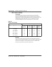
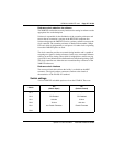
Architecture
The main functional blocks of the NTAK10 architecture include:
• DS-30X interface
• signaling interface
• three microprocessors
• digital pad.
• Card-LAN interface.
• carrier interface.
• clock controller interface.
A description of each block follows.
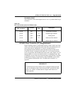
DS-30X interface
The NTAK10 interfaces to one DS-30X bus which contains 32 byte-
interleaved timeslots operating at 2.56 Mb. Each timeslot contains 10 bits in
A10 message format, 8 are assigned to voice/data (64 Kbps), one to signaling
(8 Kbps), and one is a data valid bit (8 Kbps).
Transmit data
To transmit data on the carrier, the incoming serial bit stream from the
NTAK02 circuit card is converted to 8-bit parallel bytes. The signaling bits
are extracted by the signaling interface circuitry.
Digital Pad: The parallel data is presented to the pad PROM. The PROM
contains pad values, idle code, and A/µ-law conversion. They can be set
independently for incoming and outgoing voice on a per channel basis. Four
conversion formats are provided: A-law to A-law, A-law to µ-law, µ-law to
A-law, µ-law to µ-law.