Si53xx-RM
100 Rev. 0.5
7.11.6. C1B, C2B, C3B, ALRMOUT (Si5368 [CK_CONFIG_REG = 1])
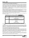
The generation of alarms on the C1B, C2B, C3B, and ALRMOUT outputs is a function of the input clock
configuration, and the frequency offset alarm enable as shown in Table 53. The LOSn_INT and FOSn_INT signals
are the raw outputs of the alarm monitors. These appear directly in the device status registers. Sticky versions of
these bits (LOSn_FLG, FOSn_FLG) drive the output interrupt and can be individually masked. Since, CKIN3 and
CKIN4 are configured as frame sync inputs (CK_CONFIG_REG = 1), ALRMOUT functions as the alignment alarm
output (ALIGN_INT) as described in Section “7.8. Frame Synchronization Realignment (Si5368 and
CK_CONFIG_REG = 1)”. The equations below assume that the output alarm is active high; however, the active
polarity is selectable via the CK_BAD_POL bit.
Operation of the C1B, C2B, C3B, and ALRMOUT pins is enabled based on setting the C1B_PIN, C2B_PIN,
C3B_PIN, and ALRMOUT_PIN register bits. Otherwise, the pin will tri-state. Also, if INT_PIN = 1, the interrupt
functionality will override the appearance of ALRMOUT at the output even if ALRMOUT_PIN =1.
Once an LOS or FOS alarm is asserted for one of the input clocks, it is held high until the input clock is validated
over a designated time period. The validation time is programmable via the VALTIME[1:0] register bits as shown in
Table 8, “AC Characteristics—All Devices”. If another error condition on the same input clock is detected during the
validation time then the alarm remains asserted and the validation time starts over.
Note that hitless switching between input clocks applies only when the input clock validation time
VALTIME[1:0] = 01 or higher.
7.11.7. LOS Algorithm for Reference Clock Input (Si5319, Si5324, Si5326, Si5327, Si5368, Si5369, Si5374,
Si5375)
The reference clock input on the XA/XB port is monitored for LOS. The LOS circuitry divides the signal at XA/XB by
128, producing a 78 kHz to 1.2 MHz signal, and monitors the signal for LOS using the same algorithm as described
in Section “7.11.1. Loss-of-Signal Alarms (Si5319, Si5324, Si5325, Si5326, Si5327, Si5367, Si5368, Si5369,
Si5374, Si5375)”. The LOSX_INT read only bit reflects the state of a loss-of-signal monitor on the XA/XB port. For
the Si5374 and Si5375, the XA/XB port refers to the OSC_P and OSC_N pins.
7.11.8. LOL (Si5319, Si5324, Si5326, Si5327, Si5368, Si5369, Si5374, Si5375)
The device has a PLL lock detection algorithm that indicates the lock status on the LOL output pin and the
LOL_INT read-only register bit. The algorithm works by continuously monitoring the phase of the input clock in
relation to the phase of the feedback clock. A retriggerable one-shot is set each time a potential phase cycle slip
condition is detected. If no potential phase cycle slip occurs for the retrigger time, the LOL output is set low,
indicating the PLL is in lock. The LOL pin is held in the active state during an internal PLL calibration. The active
polarity of the LOL output pin is set using the LOL_POL register bit (default active high).
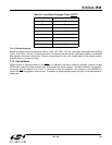
The lock detect retrigger time is user-selectable, independent of the loop bandwidth. The LOCKT[2:0] register bits
must be set by the user to the desired setting. Table 54 shows the lock detect retrigger time for both modes of
operation. LOCKT is the minimum amount of time that LOL will be active.
Table 53. Alarm Output Logic Equations [Si5368 and CKCONFIG_REG =1]
FOS_EN Alarm Output Equations
0
(Disables FOS)
C1B = LOS1_INT or (LOS3_INT and FSYNC_SWTCH_REG)
C2B = LOS2_INT or (LOS4_INT and FSYNC_SWTCH_REG)
C3B tri-state,
ALRMOUT = ALIGN_INT
1C1B = LOS1_INT or (LOS3_INT and FSYNC_SWTCH_REG) or
FOS1_INT
C2B = LOS2_INT or (LOS4_INT and FSYNC_SWTCH_REG) or
FOS2_INT
C3B tri-state,
ALRMOUT = ALIGN_INT


