Si53xx-RM
64 Rev. 0.5
6.1.3. CKOUT3 and CKOUT4 (Si5365 and Si5366)
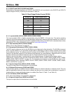
Submultiples of the output frequency on CKOUT1 and CKOUT2 can be produced on the CKOUT3 and CKOUT4
outputs using the DIV34 [1:0] control pins as shown in Table 19.
6.1.4. Loop bandwidth (Si5316, Si5322, Si5323, Si5365, Si5366)
The loop bandwidth (BW) is digitally programmable using the BWSEL [1:0] input pins. The device operating
frequency should be determined prior to loop bandwidth configuration because the loop bandwidth is a function of
the phase detector input frequency and the PLL feedback divider setting. Use DSPLLsim to calculate these values
automatically. This utility is available for download from www.silabs.com/timing.
6.1.5. Jitter Tolerance (Si5316, Si5323, Si5366)
Refer to "5.2.3. Jitter Tolerance" on page 49.
6.1.6. Narrowband Performance (Si5316, Si5323, Si5366)
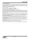
The DCO uses the reference clock on the XA/XB pins as its reference for jitter attenuation. The XA/XB pins support
either a crystal oscillator or an input buffer (single-ended or differential) so that an external oscillator can be used
as the reference source. The reference source is chosen with the RATE [1:0] pins. In both cases, there are wide
margins in the absolute frequency of the reference input because it is a fixed frequency reference and is only used
as a jitter reference and holdover reference (see "6.4. Digital Hold/VCO Freeze" on page 70).
However, care must be taken in certain areas for optimum performance. For details on this subject, refer to
"Appendix B—Frequency Plans and Jitter Performance (Si5316, Si5319, Si5323, Si5324, Si5326, Si5327, Si5366,
Si5368, Si5369, Si5374, Si5375)" on page 121. For examples of connections to the XA/XB pins, refer to "8.4.
Crystal/Reference Clock Interfaces (Si5316, Si5319, Si5323, Si5324, Si5326, Si5327, Si5366, Si5368, Si5369,
Si5374, and Si5375)" on page 113.
6.1.7. Input-to-Output Skew (Si5316, Si5323, Si5366)
The input-to-output skew for these devices is not controlled.
6.1.8. Wideband Performance (Si5322 and Si5365)
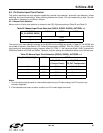
These devices operate as wideband clock multipliers without an external resonator or reference clock. They are
ideal for applications where the input clock is already low jitter and only simple clock multiplication is required. A
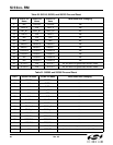
limited selection of clock multiplication factors is available (See Table 16, Table 17, and Table 18).
6.1.9. Lock Detect (Si5322 and Si5365)
A PLL loss of lock indicator is not available in these parts.
6.1.10. Input-to-Output Skew (Si5322 and Si5365)
The input-to-output skew for these devices is not controlled.
Table 19. Clock Output Divider Control (DIV34)
DIV34[1:0] Output Divider Value
HH 32
HM 16
HL 10
MH 8
MM 6
ML 5
LH 4
LM 2
LL 1


