


Si53xx-RM
Rev. 0.5 77
Because there is only one DCO and all of the outputs must be frequencies that are integer divisions of the DCO
frequency, there are restrictions on the ratio of one output frequency to another output frequency. That is, there is
considerable freedom in the ratio between the input frequency and the first output frequency; but once the first
output frequency is chosen, there are restrictions on subsequent output frequencies. These restrictions are made
tighter by the fact that the N1_HS divider is shared among all of the outputs. DSPLLsim should be used to
determine if two different simultaneous outputs are compatible with one another.
The same issue exists for inputs of different frequencies: both inputs, after having been divided by their respective
N3 dividers, must result in the same f3 frequency because the phase/frequency detector can operate at only one
frequency at one time.
7.1.2.1. Loop Bandwidth (Si5325, Si5367)
The loop bandwidth (BW) is digitally programmable using the BWSEL_REG[3:0] register bits. The device operating
frequency should be determined prior to loop bandwidth configuration because the loop bandwidth is a function of
the phase detector input frequency and the PLL feedback divider. See DSPLLsim for BWSEL_REG settings and
associated bandwidth.
7.1.2.2. Lock Detect (Si5325, Si5367)
A PLL loss of lock indicator is not available in these devices.
7.1.2.3. Input to Output Skew (Si5325, Si5367)
The input to output skew for wideband devices is not controlled.
7.1.3. Narrowband Parts (Si5319, Si5324, Si5326, Si5327, Si5368, Si5369, Si5374, Si5375)
The DCO uses the reference clock on the XA/XB pins (OSC_P and OSC_N for the Si5374 and Si5375) as its
reference for jitter attenuation. The XA/XB pins support either a crystal oscillator or an input buffer (single-ended or
differential) so that an external oscillator can become the reference source. In both cases, there are wide margins
in the absolute frequency of the reference input because it is a fixed frequency and is used only as a jitter reference
and holdover reference (see "7.6. Digital Hold" on page 87). See " Appendix A—Narrowband References" on page
119 for more details. The Si5374 and Si5375 must be used with an external crystal oscillator and cannot use
crystals.
Care must be exercised in certain areas for optimum performance. For details on this subject, refer to "Appendix
B—Frequency Plans and Jitter Performance (Si5316, Si5319, Si5323, Si5324, Si5326, Si5327, Si5366, Si5368,
Si5369, Si5374, Si5375)" on page 121. For examples of connections to the XA/XB (for the Si5374 and Si5375,
OSC_P, OSC_N) pins, refer to "8.4. Crystal/Reference Clock Interfaces (Si5316, Si5319, Si5323, Si5324, Si5326,
Si5327, Si5366, Si5368, Si5369, Si5374, and Si5375)" on page 113.
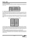
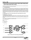
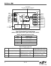
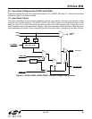
Refer to Figure 26 Narrowband PLL Divider Settings (Si5319, Si5324, Si5326, Si5327, Si5368, Si5374, Si5375), a
simplified block diagram of the device and Table 35 and Table 36 for frequency and divider limits. The PLL dividers
and their associated ranges are listed in the diagram. Each PLL divider setting is programmed by writing to device
registers. There are additional restrictions on the range of the input frequency f
IN
, the DSPLL phase detector clock
rate f3, and the DSPLL output clock f
OSC
.
The selected input clock passes through the N3 input divider and is provided to the DSPLL. In addition, the
external crystal or reference clock provides a reference frequency to the DSPLL. The DSPLL output frequency,
f
OSC
, is divided down by each output divider to generate the clock output frequencies. The input-to-output clock
multiplication ratio is defined as follows:
f
OUT
= f
IN
x N2/(N1 x N3)
where:
N1 = output divider
N2 = feedback divider
N3 = input divider