


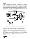
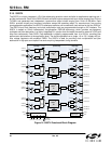
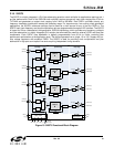
Si53xx-RM
Rev. 0.5 33
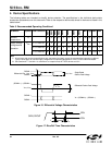
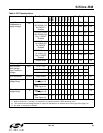
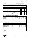
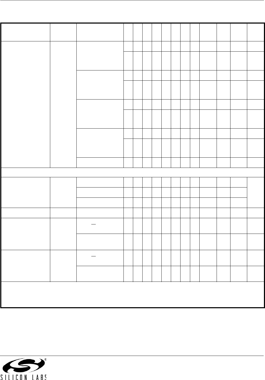
Table 4. DC Characteristics
Parameter Symbol Test Condition
Si5316
Si5322
Si5324
Si5325
Si5365
Si5366
Si5367
Si5368
Min Typ Max Units
Supply Current
(Independent of
Supply Voltage)
I
DD
LVPECL Format
622.08 MHz Out
All CKOUT’s
Enabled
— 251 279 mA
— 394 435 mA
LVPECL Format
622.08 MHz Out
Only 1 CKOUT
Enabled
— 217 243 mA
— 253 284 mA
CMOS Format
19.44 MHz Out
All CKOUTs
Enabled
— 204 234 mA
— 278 321 mA
CMOS Format
19.44 MHz Out
Only 1 CKOUT
Enabled
— 194 220 mA
— 229 261 mA
Disable Mode
—165— mA
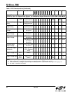
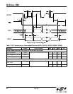
CKIN_n Input Pins
Input Common
Mode Voltage
(Input Threshold
Voltage)
V
ICM
1
1.8 V ± 10%
0.9 — 1.4 V
2.5 V ± 10%
1.0 — 1.7
3.3 V ± 10%
1.1 — 1.95
Input Resistance CKN
RIN
Single-ended
20 40 60 k
Single-Ended Input
Voltage Swing
V
ISE
f
CKIN
< 212.5 MHz
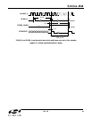
See Figure 16.
0.2 — — V
PP
f
CKIN
>212.5MHz
See Figure 16.
0.25 — — V
PP
Differential Input
Voltage Swing
V
ID
f
CKIN
< 212.5 MHz
See Figure 16.
0.2 — — V
PP
f
CKIN
>212.5MHz
See Figure 16.
0.25 — — V
PP
Notes:
1. Refer to Section 6.7.1 and 8.2.1 for restrictions on output formats for TQFP devices at 3.3 V.
2. This is the amount of leakage that the 3L inputs can tolerate from an external driver. See Figure 55 on page 115.
3. No under- or overshoot is allowed.