Si53xx-RM
Rev. 0.5 89
7.6.2. History Settings for Low Bandwidth Devices (Si5324, Si5327, Si5369, Si5374)
Because of the extraordinarily low loop bandwidth of the Si5324, Si5369 and Si5374, it is recommended that the
values for both history registers be increased for longer histories.
7.6.3. Recovery from Digital Hold (Si5319, Si5324, Si5326, Si5327, Si5368, Si5369, Si5374)
When the input clock signal returns, the device transitions from digital hold to the selected input clock. The device
performs hitless recovery from digital hold. The clock transition from digital hold to the returned input clock includes
“phase buildout” to absorb the phase difference between the digital hold clock phase and the input clock phase.
7.6.4. VCO Freeze (Si5319, Si5325, Si5367, Si5375)
If an LOS or FOS condition exists on the selected input clock, the device enters VCO freeze. In this mode, the
device provides a stable output frequency until the input clock returns and is validated. When the device enters
digital hold, the internal oscillator is initially held to the frequency value at roughly one second prior to the leading
edge of the alarm condition. VCO freeze is not compliant with SONET/SDH MTIE requirements; applications
requiring SONET/SDH MTIE requirements should use the Si5324, Si5326, Si5368, Si5369 or Si5374. Unlike the
Si5325 and Si5367, the Si5319’s VCO freeze is controlled by the XA/XB reference (which is typically a crystal)
resulting in greater stability. For the Si5319, Si5327, and Si5375, VCO freeze is similar to the Digital Hold function
of the Si5326, Si5368, and Si5369 except that the HIST_AVG and HIST_DEL registers do not exist.
7.6.5. Digital Hold versus VCO Freeze
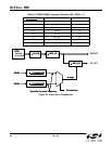
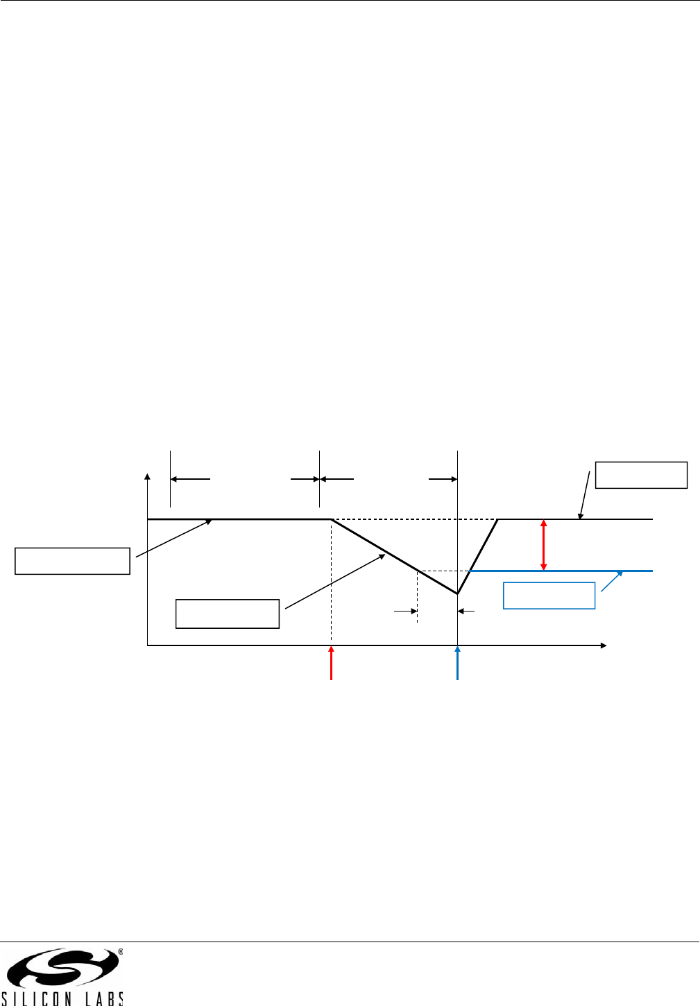
Figure 31 below is an illustration of the difference in behavior between Digital Hold and VCO Freeze.
Figure 31. Digital Hold vs. VCO Freeze Example
Normal operation
Input clock drifts
f
0
freq
LOS alarm occurs,
Start Digital hold
Digital Hold
VCO freeze
HIST_AVG HIST_DEL
Clock input
cable is pulled
time
~1 sec


