


Si53xx-RM
122 Rev. 0.5
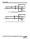
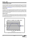
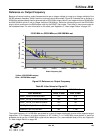
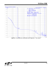
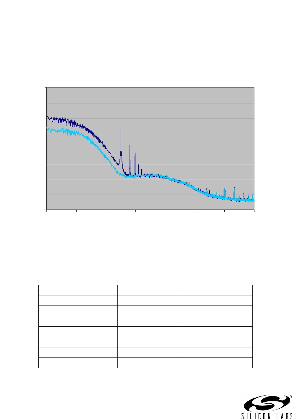
Figure 61 shows similar results and ties them to RMS jitter values. It also helps to illustrate one potential remedy
for solutions with low f3. Note that 38.88 MHz x 5 = 194.4 MHz. In this case, an FPGA was used to multiply a
38.88 MHz input clock up by a factor of five to 194.4 MHz, using a feature such as the Xilinx DCM (Digital Clock
Manager). Even though FPGAs are notorious for having jittered outputs, the jitter attenuating feature of the
Narrowband Any-Frequency Clocks allow an FPGA’s output to be used to produce a very clean clock, as can be
seen from the jitter numbers below.
Figure 61. Jitter vs. f3 with FPGA
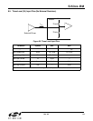
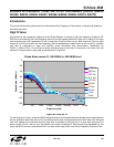
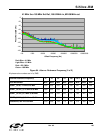
Table 61. Jitter Values for Figure 61
f3 = 3.214 kHz f3 = 16.1 kHz
CKIN = 38.88 MHz CKIN = 194.4 MHz
Jitter Bandwidth Jitter, RMS Jitter, RMS
OC-48, 12 kHz to 20 MHz 1,034 fs 285 fs
OC-192, 20 kHz to 80 MHz 668 fs 300 fs
OC-192, 4 MHz to 80 MHz 169 fs 168 fs
OC-192, 50 kHz to 80 MHz 374 fs 287 fs
800 Hz to 80 MHz 3,598 fs 378 fs
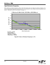
38.88 MHz in, 194.4 MHz in, 690.57 MHz out
-160
-140
-120
-100
-80
-60
-40
-20
0
10 100 1000 10000 100000 1000000 10000000 100000000
Offset Frequency (Hz)
Phase Noise (dBc/Hz)
Dark blue—38.88 MHz in, f3 = 3.214 kHz
Light blue—194.4 MHz in, f3 = 16.1 kHz