


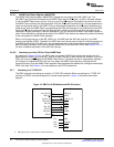

Architecture
www.ti.com
2.5.6 NAND Flash Mode
NAND Flash mode is the EMIF's third mode of operation. Each chip select space may be placed in NAND
Flash mode individually by setting the appropriate CSnNAND bit in the NAND Flash control register
(NANDFCR). Table 11 displays the bit fields present in NANDFCR and briefly describes their use.
When a chip select space is configured to operate in NAND Flash mode, the EMIF hardware can calculate
the error correction code (ECC) for each 512 byte data transfer to that chip select space. The EMIF
hardware will not generate the NAND access cycle, which includes the command, address, and data
phases, necessary to complete a transfer to NAND Flash. All NAND Flash operations can be divided into
single asynchronous cycles and with the help of software, the EMIF can execute a complete NAND
access cycle.
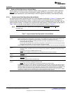
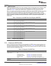
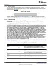
Table 11. Description of the NAND Flash Control Register (NANDFCR)
Parameter Description
CS5ECC NAND Flash ECC state for chip select 5.
• Set to 1 to start an ECC calculation.
• Cleared to 0 when NAND Flash 4 ECC register (NANDF4ECC) is read.
CS4ECC NAND Flash ECC state for chip select 4.
• Set to 1 to start an ECC calculation.
• Cleared to 0 when NAND Flash 3 ECC register (NANDF3ECC) is read.
CS3ECC NAND Flash ECC state for chip select 3.
• Set to 1 to start an ECC calculation.
• Cleared to 0 when NAND Flash 2 ECC register (NANDF2ECC) is read.
CS2ECC NAND Flash ECC state for chip select 2.
• Set to 1 to start an ECC calculation.
• Cleared to 0 when NAND Flash 1 ECC register (NANDF1ECC) is read.
CS5NAND NAND Flash mode for chip select 5.
• Set to 1 to enable NAND Flash mode.
CS4NAND NAND Flash mode for chip select 4.
• Set to 1 to enable NAND Flash mode.
CS3NAND NAND Flash mode for chip select 3.
• Set to 1 to enable NAND Flash mode.
CS2NAND NAND Flash mode for chip select 2.
• Set to 1 to enable NAND Flash mode.
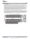
2.5.6.1 Configuring for NAND Flash Mode
Similar to the asynchronous accesses previously described, the EMIF's memory-mapped registers must
be programmed appropriately to interface to a NAND Flash device. Table 12 lists the bit fields that must
be programmed when operating in NAND Flash mode and the values to set each bit. NAND Flash mode
cannot be used with Extended Wait mode.
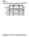
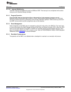
Table 12. Configuration For NAND Flash
Register Bit Field Configuration Value
Asynchronous configuration SS 0
register (ACFGn)
EW 0
W_SETUP/R_SETUP See Section 3.2 for information on how to program.
W_STROBE/R_STROBE See Section 3.2 for information on how to program.
W_HOLD/R_HOLD See Section 3.2 for information on how to program.
ASIZE Programmed to equal the width of the NAND Flash device
NAND Flash control register CS2NAND 1
(NANDFCR)
22
Asynchronous External Memory Interface (EMIF) SPRUEQ7C–February 2010
Submit Documentation Feedback
Copyright © 2010, Texas Instruments Incorporated