CLE_EM_A[16]
ALE_EM_A[17]
EM_CS[n]
EM_WE
EM_OE
EM_D[7:0]
EM_WAIT[n]
EMIF
CLE
ALE
CE
WE
OE
IO[7:0]
R/B
NAND flash
a) Connection to 8-bit NAND device
b) Connection to 16-bit NAND device
EM_WAIT[n]
EM_D[15:0]
EM_OE
EM_WE
EM_CS[n]
ALE_EM_A[17]
CLE_EM_A[16]
EMIF
CE
IO[15:0]
R/B
OE
WE
NAND flash
CLE
ALE
www.ti.com
Architecture
2.5.6.2 Connecting to NAND Flash
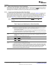
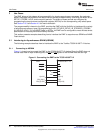
Figure 8 shows the EMIF external pins used to interface with a NAND Flash device. EMIF address lines
are used to drive the NAND Flash device's command latch enable (CLE) and address latch enable (ALE)
signals.
NOTE: The EMIF will not control the NAND Flash device's write protect pin. The write protect pin
must be controlled outside of the EMIF.
Figure 8. EMIF to NAND Flash Interface
2.5.6.3 Driving CLE and ALE
As stated in Section 2.5.1, the EMIF always drives the least significant bit of a 32-bit word address on
EM_A[0]. This functionality must be considered when attempting to drive the address lines connected to
CLE and ALE to the appropriate state.
For example, if using EM_A[2] and EM_A[1] to connect to CLE and ALE, respectively, the following offsets
should be chosen:
• 00h to drive CLE and ALE low
• 10h to drive CLE high and ALE low
• 0Bh to drive CLE low and ALE high
These offsets should be added to the base address for the chip select space the NAND Flash device is
connected to. For example, if the base address of the CS space the NAND Flash device is connected to is
4200 0000h, then the above list translates to the following memory-mapped addresses: 4200 0000h, 4200
0010h, and 4200 000Bh, respectively. Therefore, when attempting to drive CLE high and ALE low, the
memory-mapped address of 4200 0010h would be written to.
23
SPRUEQ7C–February 2010 Asynchronous External Memory Interface (EMIF)
Submit Documentation Feedback
Copyright © 2010, Texas Instruments Incorporated


