


www.ti.com
Use Cases
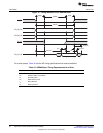
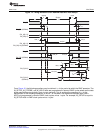
Since the value of the W_SETUP/R_SETUP, W_STROBE/R_STROBE, W_HOLD/R_HOLD, and TA fields
are equal to EMIF clock cycles minus 1 cycle, the A2CR should be configured as in Table 23. In this
example, the EM_WAIT signal is not implemented; therefore, the asynchronous wait cycle configuration
register (AWCCR) does not need to be programmed.
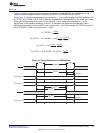
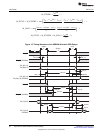
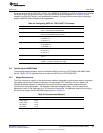
Table 23. Configuring A2CR for TC5516100FT-12 Example
Parameter Setting
SS Select Strobe mode.
• SS = 0. Places EMIF in Normal Mode.
EW Extended Wait mode enable.
• EW = 0. Disabled Extended wait mode.
W_SETUP/R_SETUP Read/Write setup widths.
• W_SETUP = 0
• R_SETUP = 0
W_STROBE/R_STROBE Read/Write strobe widths.
• W_STROBE = 0
• R_STROBE = 0
W_HOLD/R_HOLD Read/Write hold widths.
• W_HOLD = 0
• R_HOLD = 0
TA Minimum turnaround time.
• TA = 0
ASIZE Asynchronous Device Bus Width.
• ASIZE = 1, select a 16-bit data bus width
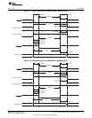
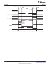
3.2 Interfacing to NAND Flash
The following example explains how to interface the EMIF to the Hynix HY27UA081G1M NAND Flash
device. Section 2.5.6.2 describes how to connect the EMIF to the HY27UA081G1M.
3.2.1 Margin Requirements
The Flash interface is typically a low-performance interface compared to synchronous memory interfaces,
high-speed asynchronous memory interfaces, and high-speed FIFO interfaces. For this reason, this
example gives little attention to minimizing the amount of margin required when programming the
asynchronous timing parameters. The approach used requires approximately 10 ns of margin on all
parameters, which is not significant for a 100-ns read or write cycle. For additional details on minimizing
the amount of margin, see the ASRAM example given in Section 3.1.
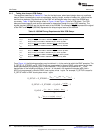
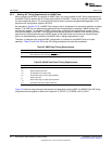
Table 24. Recommended Margins
Timing Parameter Recommended Margin
Output Setup 10 nS
Output Hold 10 nS
Input Setup 10 nS
Input Hold 10 nS
39
SPRUEQ7C–February 2010 Asynchronous External Memory Interface (EMIF)
Submit Documentation Feedback
Copyright © 2010, Texas Instruments Incorporated