


www.ti.com
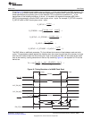
Use Cases
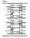
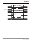
3.2.3 Example Using Hynix HY27UA081G1M
This section takes you through the configuration steps required to implement Hynix’s HY27UA081G1M
NAND Flash with the EMIF. The following assumptions are made:
• NAND Flash is connected to chip select space 2 (EM_CS[2])
• EMIF clock speed is 100 MHZ (t
cyc
= 10 nS)
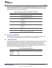
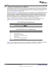
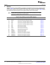
Table 28 lists the data sheet specifications for the EMIF and Table 29 lists the data sheet specifications
for the NAND Flash.
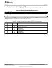
Table 28. EMIF Timing Requirements for HY27UA081G1M Example
Parameter Description Min Max Units
t
SU
Data Setup time, data valid before EM_OE high 5 nS
t
H
Data Hold time, data valid after EM_OE high 0 nS
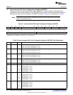
Table 29. NAND Flash Timing Requirements for HY27UA081G1M Example
Parameter Description Min Max Units
t
RP
Read Pulse width 60 nS
t
REA
Read Enable Access time 60 nS
t
CEA
Chip Enable low to output valid 75 nS
t
CHZ
Chip Enable high to output High-impedance 20 nS
t
RC
Read Cycle time 80 nS
t
RHZ
Read Enable high to output High-impedance 30 nS
t
CLR
Command Latch low to Read enable low 10 nS
t
WP
Write Pulse width 60 nS
t
CLS
CLE Setup time 0 nS
t
ALS
ALE Setup time 0 nS
t
CS
CS Setup time 0 nS
t
DS
Data Setup time 20 nS
t
CLH
CLE Hold time 10 nS
t
ALH
ALE Hold time 10 nS
t
CH
CS Hold time 10 nS
t
DH
Data Hold time 10 nS
t
WC
Write Cycle time 80 nS
45
SPRUEQ7C–February 2010 Asynchronous External Memory Interface (EMIF)
Submit Documentation Feedback
Copyright © 2010, Texas Instruments Incorporated