


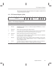

PCI Configuration Registers
A-8
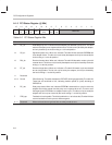
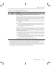
This register holds the base address for ThunderLAN’s register set in I/O
space. Bit 0 of this register is hardwired to a 1 to indicate that this is a memory-
mapped base address. Bits 1 through 3 are hardwired to 0 to indicate that the
register set occupies four 32-bit words.
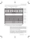
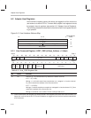
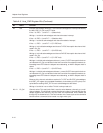
A.1.13 PCI Memory Base Address Register (@ 14h)
16171819202122232425262728293031
Memory Base Address 16 MSBs
000Memory Base Address 12 LSBs
0123456789101112131415
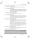
16171819202122232425262728293031
0000
0123456789101112131415
This register holds the base address for ThunderLAN’s register set in memory
space. Bit 0 of this register is hardwired to a 0 to indicate that this is a memory-
mapped base address. Bits 1 and 2 are hardwired to 0 to indicate that the regis-
ter set can be located anywhere in 32-bit address space. Bit 3 of this register
(prefetchable bit) is hardwired to a 0, indicating that prefetching is not allowed.
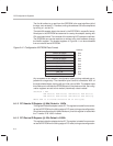
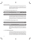
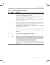
A.1.14 PCI BIOS ROM Base Address Register (@ 30h)
Reserved
16171819202122232425262728293031
BIOS ROM Base Address 16 MSBs
BRE
0123456789101112131415
This register holds the base address for ThunderLAN’s BIOS ROM in memory
space. Bit 0, BRE, is an enable bit for BIOS ROM accesses. When set to a 1,
BIOS ROM accesses are enabled; when set to a 0 they are disabled. (The
Mem_En in the PCI command register must also be set to allow BIOS ROM
accesses.)
A.1.15 PCI NVRAM Register (@ 34h)
This register allows configuration space access to the external EEPROM, in
addition to the normal DIO space access through the NetSio register. Control
of the EEPROM interface swaps between these two control registers on a
most-recently-written basis. Whenever the PCI NVRAM register is written to,
it takes control of the EEPROM interface pins. Whenever the DIO_DATA regis-
ter is written to, the NetSio register takes control of the EEPROM interface