


B-2 SYNCHRONIZATION OF DIGITAL FACILITIES
_ ___________________________________________________________________________________________________________________________
_ ___________________________________________________________________________________________________________________________
_ ___________________________________________________________________________________________________________________________
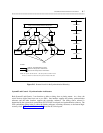
systems connected by T1-carrier facilities. For this arrangement, the transmitting portion of each channel
bank independently determines the clock rates. The receiving portion of each channel bank derives its
clock from the incoming digital bit stream. In this arrangement, the channel banks convert the received
digital signal directly to analog, and there is no requirement that the two clock frequencies precisely match
as the channel bank does not interface to another digital system.
. . . . . . . . . . . . . . . . . . . . . . . . . . . . . . . . . . . . . . . . . . . . . . . . . . . . . . . . . . . . . . . . . . . . . . . . . . . . . . . . . . . . . . . . . . . . . . . . . . . . . . . . . . . . . . . . . . . . . . . . . . . . . . . . . . . . . . . . . . . . . . .
. . . . . . . . . . . . . . . . . . . . . . . . . . . . . . . . . . . . . . . . . . . . . . . . . . . . . . . . . . . . . . . . . . . . . . . . . . . . . . . . . . . . . . . . . . . . . . . . . . . . . . . . . . . . . . . . . . . . . . . . . . . . . . . . . . . . . . . . . . . . . .
F
0
F
0
F
0
F
0
F
1
F
0
DIGITAL BIT STREAM
DIGITAL BIT STREAM
CHANNEL
BANK
CHANNEL
BANK
CHANNEL
BANK
DIGITAL
SWITCHING
SYSTEM
F
0
DIGITAL
SWITCHING
SYSTEM
F
0
DIGITAL
SWITCHING
SYSTEM
F
0
RECEIVE
RECEIVE
RECEIVE
TRANSMIT
F
1
TRANSMIT
F
0
TRANSMIT
F
0
TRANSMIT
TRANSMIT
TRANSMIT
RECEIVE
RECEIVE
RECEIVE
DIGITAL BIT STREAM
ANALOG ANALOG
DIGITAL DIGITAL
DIGITAL DIGITAL
REFERENCE
CLOCK RATE F
0
REFERENCE
CLOCK RATE F
0
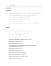
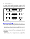
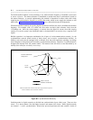
C: Externally Synced
B: Loop Timed
A: Not Synced
Figure B-1. Options for Synchronization
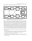
Figure B-1-B, Options for Synchronization, shows a different connection between a channel bank and a
digital switching system. For this configuration, the digital switch transmits a digital bit stream at the rate
(F0) that is determined by its internal clock. The digital switch must receive the incoming digital bit stream
at this same rate (F0). Otherwise, the switch’s receiving buffer may eventually overrun or underrun.
NOTE: Switching is done by placing the signals from individual time slots on one link into the time
slots on other links using a process called time-slot interchange (TSI). For this process to work
properly, bit synchronization must be maintained on all links terminating on the digital switching node,
no matter where the links originate.
If the average transmit rate is faster than the average receive rate, the receive buffer will eventually overrun.
If the average receive bit-clock rate is faster than the average transmit bit-clock rate, the receive buffer will
eventually underrun. It is necessary to prevent overruns (deletions) and underruns (repetitions) by
synchronizing the network properly. Improper synchronization results in buffers repeating or deleting bits
in 1-frame increments.
NOTE: The deletion or repetition of a single frame is termed a slip or a controlled slip. For an
individual digital bit stream, slips are serious impairments since digital switching systems with
improperly synchronized clocks will eventually suffer slips on every received digital bit stream.