CY7C63310, CY7C638xx
enCoRe™ II
Low Speed USB Peripheral Controller
Cypress Semiconductor Corporation • 198 Champion Court • San Jose
,
CA 95134-1709 • 408-943-2600
Document 38-08035 Rev. *K Revised December 08 2008
1. Features
■
USB 2.0-USB-IF certified (TID # 40000085)
■
enCoRe™ II USB - “enhanced Component Reduction”
❐
Crystalless oscillator with support for an external clock. The
internal oscillator eliminates the need for an external crystal
or resonator.
❐
Two internal 3.3V regulators and an internal USB pull up
resistor
❐
Configurable IO for real world interface without external com-
ponents
■
USB Specification compliance
❐
Conforms to USB Specification, Version 2.0
❐
Conforms to USB HID Specification, Version 1.1
❐
Supports one low speed USB device address
❐
Supports one control endpoint and two data endpoints
❐
Integrated USB transceiver with dedicated 3.3V regulator for
USB signalling and D– pull up.
■
Enhanced 8-bit microcontroller
❐
Harvard architecture
❐
M8C CPU speed is up to 24 MHz or sourced by an external
clock signal
■
Internal memory
❐
Up to 256 bytes of RAM
❐
Up to eight Kbytes of Flash including EEROM emulation
■
Interface can auto configure to operate as PS/2 or USB
❐
No external components for switching between PS/2 and
USB modes
❐
No General Purpose IO (GPIO) pins required to manage dual
mode capability
■
Low power consumption
❐
Typically 10 mA at 6 MHz
❐
10 μA sleep
■
In system reprogrammability:
❐
Allows easy firmware update
■
GPIO ports
❐
Up to 20 GPIO pins
❐
2 mA source current on all GPIO pins. Configurable 8 or
50 mA/pin current sink on designated pins.
❐
Each GPIO port supports high impedance inputs, config-
urable pull up, open drain output, CMOS/TTL inputs, and
CMOS output
❐
Maskable interrupts on all IO pins
■
A dedicated 3.3V regulator for the USB PHY. Aids in signalling
and D– line pull up
■
125 mA 3.3V voltage regulator powers external 3.3V devices
■
3.3V IO pins
❐
4 IO pins with 3.3V logic levels
❐
Each 3.3V pin supports high impedance input, internal pull
up, open drain output or traditional CMOS output
■
SPI serial communication
❐
Master or slave operation
❐
Configurable up to 4 Mbit/second transfers in the master
mode
❐
Supports half duplex single data line mode for optical sensors
■
2-channel 8-bit or 1-channel 16-bit capture timer registers.
Capture timer registers store both rising and falling edge times.
❐
Two registers each for two input pins
❐
Separate registers for rising and falling edge capture
❐
Simplifies the interface to RF inputs for wireless applications
■
Internal low power wakeup timer during suspend mode:
❐
Periodic wakeup with no external components
■
12-bit Programmable Interval Timer with interrupts
■
Advanced development tools based on Cypress PSoC® tools
■
Watchdog timer (WDT)
■
Low voltage detection with user configurable threshold
voltages
■
Operating voltage from 4.0V to 5.5V DC
■
Operating temperature from 0–70°C
■
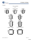
Available in 16 and 18-pin PDIP; 16, 18, and 24-pin SOIC;
24-pin QSOP, and 32-pin QFN packages
■
Industry standard programmer support
1.1 Applications
The CY7C63310/CY7C638xx is targeted for the following
applications:
■
PC HID devices
❐
Mice (optomechanical, optical, trackball)
■
Gaming
❐
Joysticks
❐
Game pad
■
General purpose
❐
Barcode scanners
❐
POS terminal
❐
Consumer electronics
❐
Toys
❐
Remote controls
❐
Security dongles
[+] Feedback [+] Feedback


