CY7C63310, CY7C638xx
Document 38-08035 Rev. *K Page 35 of 83
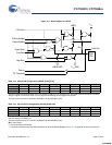
14.2 GPIO Port Configuration
All the GPIO configuration registers have common configuration
controls. The following are the bit definitions of the GPIO
configuration registers.
14.2.1 Int Enable
When set, the Int Enable bit allows the GPIO to generate
interrupts. Interrupt generate can occur regardless of whether
the pin is configured for input or output. All interrupts are edge
sensitive; however for any interrupt that is shared by multiple
sources (that is, Ports 2, 3, and 4) all inputs must be deasserted
before a new interrupt can occur.
When clear, the corresponding interrupt is disabled on the pin.
It is possible to configure GPIOs as outputs, enable the interrupt
on the pin and then generate the interrupt by driving the appro-
priate pin state. This is useful in tests and may have value in
applications.
14.2.2 Int Act Low
When set, the corresponding interrupt is active on the falling
edge.
When clear, the corresponding interrupt is active on the rising
edge.
14.2.3 TTL Thresh
When set, the input has TTL threshold. When clear, the input has
standard CMOS threshold.
14.2.4 High Sink
When set, the output can sink up to 50 mA.
When clear, the output can sink up to 8 mA.
Only the P1.7–P1.3 have 50 mA sink drive capability. Other pins
have 8 mA sink drive capability.
14.2.5 Open Drain
When set, the output on the pin is determined by the Port Data
Register. If the corresponding bit in the Port Data Register is set,
the pin is in high impedance state. If the corresponding bit in the
Port Data Register is clear, the pin is driven low.
When clear, the output is driven LOW or HIGH.
14.2.6 Pull up Enable
When set the pin has a 7K pull up to V
CC
(or VREG for ports with
V3.3 enabled).
When clear, the pull up is disabled.
14.2.7 Output Enable
When set, the output driver of the pin is enabled.
When clear, the output driver of the pin is disabled.
For pins with shared functions there are some special cases.
14.2.8 VREG Output/SPI Use
The P1.2(VREG), P1.3(SSEL), P1.4(SCLK), P1.5(SMOSI) and
P1.6(SMISO) pins are used for their dedicated functions or for
GPIO.
To enable the pin for GPIO, clear the corresponding VREG
Output or SPI Use bit. The SPI function controls the output
enable for its dedicated function pins when their GPIO enable bit
is clear. The VREG output is not available on the CY7C63801
and CY7C63310.
14.2.9 3.3V Drive
The P1.3(SSEL), P1.4(SCLK), P1.5(SMOSI) and P1.6(SMISO)
pins have an alternate voltage source from the voltage regulator.
If the 3.3V Drive bit is set a high level is driven from the voltage
regulator instead of from V
CC
.
Setting the 3.3V Drive bit does not enable the voltage regulator.
That must be done explicitly by setting the VREG Enable bit in
the VREGCR Register (Table 19-1 on page 57).
[+] Feedback [+] Feedback


