CY7C63310, CY7C638xx
Document 38-08035 Rev. *K Page 68 of 83
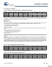
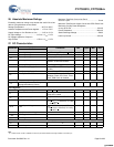
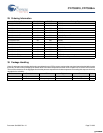
26. Absolute Maximum Ratings
Exceeding maximum ratings may shorten the useful life of the
device. User guidelines are not tested.
Storage Temperature ................................... –40°C to +90°C
Ambient Temperature with Power Applied..... –0°C to +70°C
Supply Voltage on V
CC
Relative to V
SS
..........–0.5V to +7.0V
DC Input Voltage ................................–0.5V to + V
CC
+ 0.5V
DC Voltage Applied to Outputs in
High-Z State....................................... –0.5V to + V
CC
+ 0.5V
Maximum Total Sink Current into Port 0
and Port 1 pins ............................................................ 70 mA
Maximum Total Source Output Current into GPIO Pins30 mA
Maximum On-chip Power Dissipation
on any GPIO Pin......................................................... 50 mW
Power Dissipation .................................................... 300 mW
Static Discharge Voltage ............................................. 2200V
Latch Up Current ..................................................... 200 mA
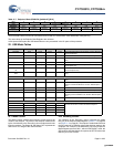
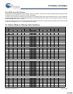
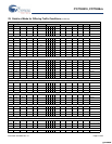
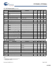
27. DC Characteristics
Parameter
Description
Conditions Min Typical Max Unit
General
V
CC1
Operating Voltage No USB activity, CPU speed < 12 MHz 4.0 5.5 V
V
CC2
Operating Voltage USB activity, CPU speed < 12 MHz 4.35 5.25 V
V
CC3
Operating Voltage Flash programming 4.0 5.5 V
V
CC4
Operating Voltage No USB activity, CPU speed is
between 12 MHz and 24 MHz
4.75 5.5 V
T
FP
Operating Temp Flash Programming 0 70 °C
I
CC1
V
CC
Operating Supply Current V
CC
= 5.25V, no GPIO loading,
24 MHz
40 mA
I
CC2
V
CC
Operating Supply Current V
CC
= 5.0V, no GPIO loading, 6 MHz 10 mA
I
SB1
Standby Current Internal and External Oscillators,
Bandgap, Flash, CPU Clock, Timer
Clock, USB Clock all disabled
10 μA
Low Voltage Detect
V
LVD
Low-Voltage Detect Trip Voltage
(8 programmable trip points)
2.681 4.872 V
3.3V Regulator
I
VREG
Max Regulator Output Current 4.35V < V
CC
< 5.5V 125 mA
I
KA
Keep Alive Current When regulator is disabled with
“keep alive” enable
20 μA
V
KA
Keep Alive Voltage Keep alive bit set in VREGCR 2.35 3.8 V
V
REG1
V
REG
Output Voltage V
CC
> 4.35V, 0 < temp < 40°C,
25 mA <
I
VREG
< 125 mA (3.3V ± 8%)
T = 0 to 70C
3.0 3.6 V
V
REG2
V
REG
Output Voltage V
CC
> 4.35V, 0 < temp < 40°C,
1 mA <
I
VREG
< 25 mA (3.3V ± 4%)
T = 0 to 40°C
3.15 3.45 V
C
LOAD
Capacitive load on Vreg pin 1 2 μF
LN
REG
Line Regulation 1%/V
LD
REG
Load Regulation 0.04 %/mA
USB Interface
V
ON
Static Output High 15K ± 5% Ohm to V
SS
2.8 3.6 V
V
OFF
Static Output Low R
UP
is enabled 0.3 V
Note
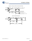
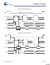
6. In Master mode, first bit is available 0.5 SPICLK cycle before Master clock edge available on the SCLK pin.
[+] Feedback [+] Feedback


