CY7C63310, CY7C638xx
Document 38-08035 Rev. *K Page 36 of 83
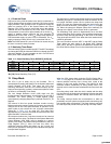
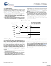
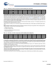
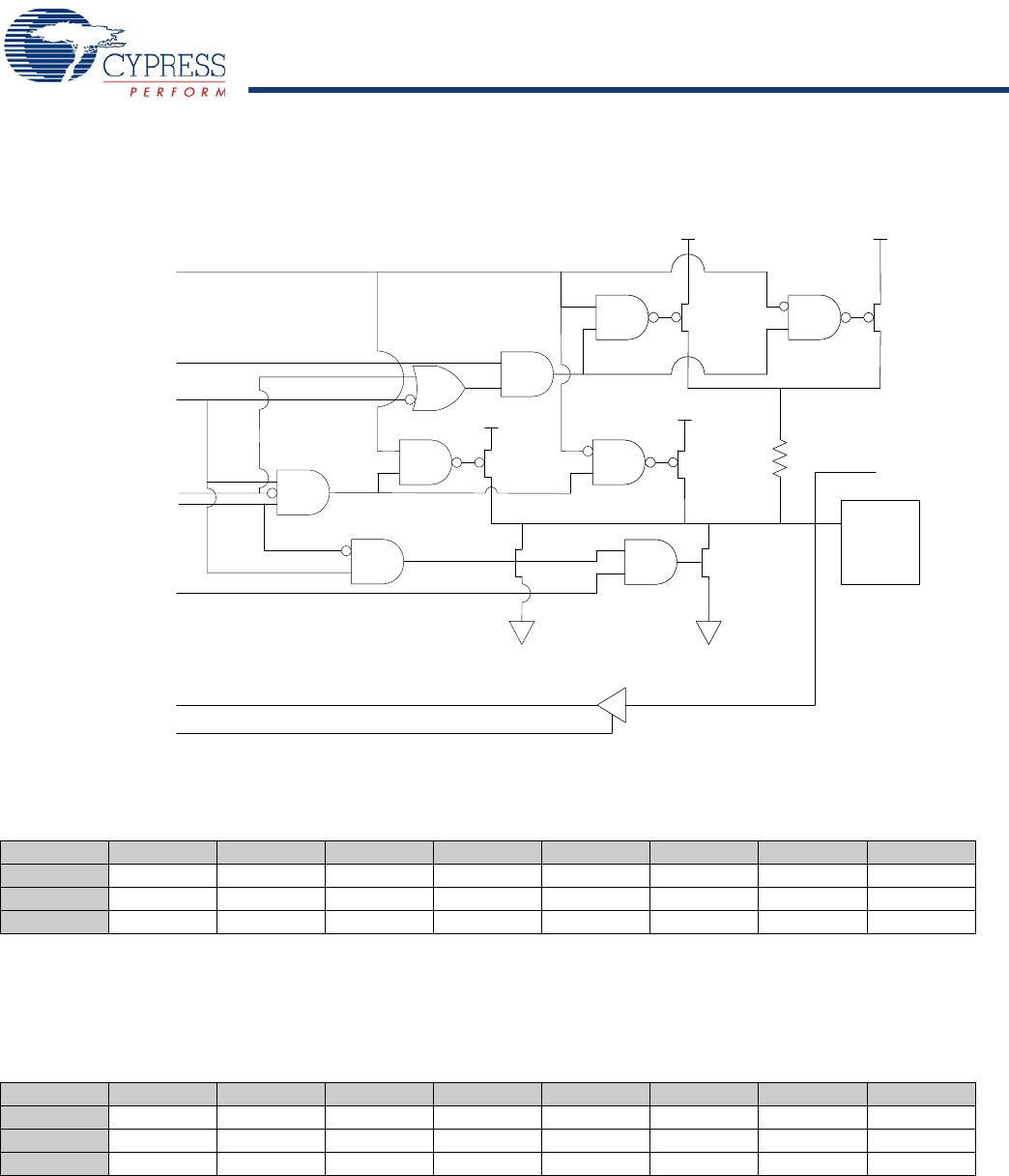
Figure 14-1. Block Diagram of a GPIO
V
CC
VREG
V
CC
VREG
GPIO
PIN
R
UP
Data Out
V
CC
GND
VREG
GND
3.3V Drive
Pull-Up Enable
Output Enable
Open Drain
Port Data
High Sink
Data In
TTL Threshold
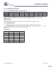
Table 14-5. P0.0/CLKIN Configuration (P00CR) [0x05] [R/W]
Bit # 7 6 5 4 3 2 1 0
Field Reserved Int Enable Int Act Low TTL Thresh Reserved Open Drain Pull up Enable Output Enable
Read/Write -- R/W R/W R/W -- R/W R/W R/W
Default 0 0 0 0 000 0
This pin is shared between the P0.0 GPIO use and the CLKIN pin for an external clock. When the external clock input is enabled
(Bit[0] in register CPUCLKCR Table 10-3 on page 22) the settings of this register are ignored.
The use of the pin as the P0.0 GPIO is available in all the enCoRe II parts.
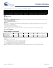
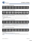
Table 14-6. P0.1/CLKOUT Configuration (P01CR) [0x06] R/W]
Bit # 7 6 5 4 3 2 1 0
Field CLK Output Int Enable Int Act Low TTL Thresh Reserved Open Drain Pull Up Enable Output Enable
Read/Write R/W R/W R/W R/W -- R/W R/W R/W
Default 0 0 0 0 000 0
This pin is shared between the P0.1 GPIO use and the CLKOUT pin. When CLK output is set, the internally selected clock is
sent out onto P0.1CLKOUT pin.
The use of the pin as the P0.1 GPIO is available in all the enCoRe II parts.
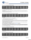
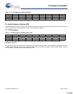
Bit 7: CLK Output
0 = The clock output is disabled.
1 = The clock selected by the CLK Select field (Bit [1:0] of the CLKIOCR Register (Table 10-7 on page 26) is driven out to the pin.
[+] Feedback [+] Feedback


