CY7C63310, CY7C638xx
Document 38-08035 Rev. *K Page 21 of 83
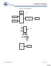
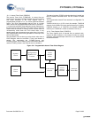
10.1 Clock Architecture Description
The enCoRe II clock selection circuitry allows the selection of
independent clocks for the CPU, USB, Interval Timers and
Capture Timers.
The CPU clock CPUCLK is sourced from an external clock or the
Internal 24 MHz Oscillator. The selected clock source is
optionally divided by 2
n
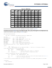
, where n is 0-5,7 (see Table 10-4 on page
23).
USBCLK, which must be 12 MHz for the USB SIE to function
properly, is sourced by the Internal 24 MHz Oscillator or an
external 12 MHz/24 MHz clock. An optional divide by two allows
the use of 24 MHz source.
The Interval Timer clock (ITMRCLK), is sourced from an external
clock, the Internal 24 MHz Oscillator, the Internal 32 kHz low
power oscillator, or from the timer capture clock (TCAPCLK). A
programmable prescaler of 1, 2, 3, 4 then divides the selected
source.
The Timer Capture clock (TCAPCLK) is sourced from an external
clock, Internal 24 MHz Oscillator, or the Internal 32 kHz low
power oscillator.
The CLKOUT pin (P0.1) is driven from one of many sources. This
is used for test and is also used in some applications. The
sources that drive the CLKOUT follow:
■
CLKIN after the optional EFTB filter
■
Internal 24 MHz Oscillator
■
Internal 32 kHz low power oscillator
■
CPUCLK after the programmable divider
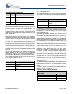
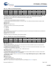
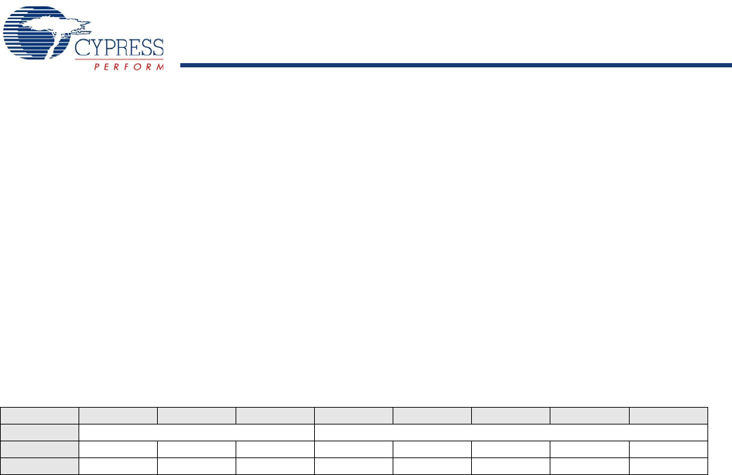
Table 10-1. IOSC Trim (IOSCTR) [0x34] [R/W]
Bit # 7 6 5 4 3 2 1 0
Field foffset[2:0] Gain[4:0]
Read/Write R/W R/W R/W R/W R/W R/W R/W R/W
Default 0 0 0 D D D D D
The IOSC Calibrate register calibrates the internal oscillator. The reset value is undefined but during boot the SROM writes a
calibration value that is determined during manufacturing test. This value does not require change during normal use. This is
the meaning of ‘D’ in the Default field.
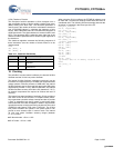
Bit [7:5]: foffset [2:0]
This value is used to trim the frequency of the internal oscillator. These bits are not used in factory calibration and are zero.
Setting each of these bits causes the appropriate fine offset in oscillator frequency.
foffset bit 0 = 7.5 kHz
foffset bit 1 = 15 kHz
foffset bit 2 = 30 kHz
Bit [4:0]: Gain [4:0]
The effective frequency change of the offset input is controlled through the gain input. A lower value of the gain setting increases
the gain of the offset input. This value sets the size of each offset step for the internal oscillator. Nominal gain change
(kHz/offsetStep) at each bit, typical conditions (24 MHz operation):
Gain bit 0 = –1.5 kHz
Gain bit 1 = –3.0 kHz
Gain bit 2 = –6 kHz
Gain bit 3 = –12 kHz
Gain bit 4 = –24 kHz
[+] Feedback [+] Feedback


