CY7C63310, CY7C638xx
Document 38-08035 Rev. *K Page 60 of 83
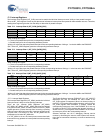
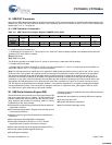
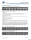
21.4 Endpoint 1 and 2 Mode
Table 21-4. Endpoint 1 and 2 Mode (EP1MODE – EP2MODE) [0x45, 0x46] [R/W]
Bit # 7 6 5 4 3 2 1 0
Field Stall Reserved NAK Int Enable ACK’d
Transaction
Mode[3:0]
Read/Write R/W R/W R/W R/C (Note 4) R/W R/W R/W R/W
Default 0 0 0 0 000 0
Bit 7: Stall
When this bit is set the SIE stalls an OUT packet if the Mode Bits are set to ACK-OUT, and the SIE stalls an IN packet if the
mode bits are set to ACK-IN. This bit must be clear for all other modes
Bit 6: Reserved
Bit 5: NAK Int Enable
This bit when set causes an endpoint interrupt to be generated even when a transfer completes with a NAK. Unlike enCoRe,
enCoRe II family members do not generate an endpoint interrupt under these conditions unless this bit is set.
0 = Disable interrupt on NAK’d transactions
1 = Enable interrupt on NAK’d transaction
Bit 4: ACK’d Transaction
The ACK’d transaction bit is set when the SIE engages in a transaction to the register’s endpoint that completes with an ACK
packet.
This bit is cleared by any writes to the register.
0 = The transaction does not complete with an ACK
1 = The transaction completes with an ACK
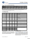
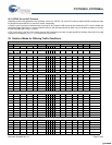
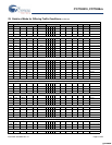
Bit [3:0]: Mode [3:0]
The endpoint modes determine how the SIE responds to USB traffic that the host sends to the endpoint. The mode controls how
the USB SIE responds to traffic, and how the USB SIE changes the mode of that endpoint as a result of host packets to the
endpoint.
Note When the SIE writes to the EP1MODE or the EP2MODE register, it blocks firmware writes to the EP2MODE or the
EP1MODE registers respectively (if both writes occur in the same clock cycle). This is because the design employs only one
common ‘update’ signal for both EP1MODE and EP2MODE registers. As a result, when SIE writes to say EP1MODE register,
the update signal is set and this prevents firmware writes to EP2MODE register. SIE writes to the endpoint mode registers have
higher priority than firmware writes. This mode register write block situation can put the endpoints in incorrect modes. Firmware
must read the EP1/2MODE registers immediately following a firmware write and rewrite if the value read is incorrect.
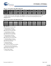
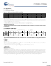
Table 21-5. Endpoint 0 Data (EP0DATA) [0x50-0x57] [R/W]
Bit # 7 6 5 4 3 2 1 0
Field Endpoint 0 Data Buffer [7:0]
Read/Write R/W R/W R/W R/W R/W R/W R/W R/W
Default Unknown Unknown Unknown Unknown Unknown Unknown Unknown Unknown
The Endpoint 0 buffer is comprised of 8 bytes located at address 0x50 to 0x57.
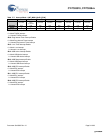
Table 21-6. Endpoint 1 Data (EP1DATA) [0x58-0x5F] [R/W]
Bit # 7 6 5 4 3 2 1 0
Field Endpoint 1 Data Buffer [7:0]
Read/Write R/W R/W R/W R/W R/W R/W R/W R/W
Default Unknown Unknown Unknown Unknown Unknown Unknown Unknown Unknown
The Endpoint 1 buffer is comprised of 8 bytes located at address 0x58 to 0x5F.
[+] Feedback [+] Feedback


