


CY7C63310, CY7C638xx
Document 38-08035 Rev. *K Page 34 of 83
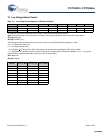
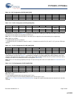
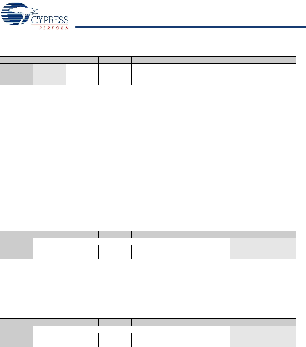
Table 14-2. P1 Data Register (P1DATA) [0x01] [R/W]
Bit # 7 6 5 4 3 2 1 0
Field P1.7 P1.6/SMISO P1.5/SMOSI P1.4/SCLK P1.3/SSEL P1.2/VREG P1.1/D– P1.0/D+
Read/Write R/W R/W R/W R/W R/W R/W R/W R/W
Default 0 0 0 0 0 0 0 0
This register contains the data for Port 1. Writing to this register sets the bit values to be output on output enabled pins. Reading
from this register returns the current state of the Port 1 pins.
Bit 7: P1.7 Data
P1.7 only exists in the CY7C638xx.
Bit [6:3]: P1.6–P1.3 Data/SPI Pins (SMISO, SMOSI, SCLK, SSEL)
Besides their use as the P1.6–P1.3 GPIOs, these pins are also used for the alternate function as the SPI interface pins. To
configure the P1.6–P1.3 pins, refer to the P1.3–P1.6 Configuration Register (Table 14-13 on page 39).
The use of the pins as the P1.6–P1.3 GPIOs and the alternate functions exist in all the enCoRe II parts.
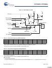
Bit 2: P1.2/VREG
On the CY7C638x3, this pin is used as the P1.2 GPIO or the VREG output. If the VREG output is enabled (Bit 0
Table 19-1 on page 57 is set), a 3.3V source is placed on the pin and the GPIO function of the pin is disabled.
The VREG functionality is not present in the CY7C63310 and the CY7C63801 variants. A 1 μF min, 2 μF max capacitor is
required on VREG output.
Bit [1:0]: P1.1–P1.0/D– and D+
When the USB mode is disabled (Bit 7 in Table 21-1 on page 58 is clear), the P1.1 and P1.0 bits are used to control the state of
the P1.0 and P1.1 pins. When the USB mode is enabled, the P1.1 and P1.0 pins are used as the D– and D+ pins respectively.
If the USB Force State bit (Bit 0 in Table 19-1) is set, the state of the D– and D+ pins are controlled by writing to the D– and D+ bits.
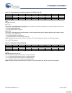
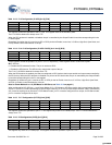
Table 14-3. P2 Data Register (P2DATA) [0x02] [R/W]
Bit # 7 6 5 4 3 2 1 0
Field Reserved P2.1–P2.0
Read/Write - - - - - - R/W R/W
Default 0 0 0 0 0 0 0 0
This register contains the data for Port 2. Writing to this register sets the bit values to output on output enabled pins. Reading
from this register returns the current state of the Port 2 pins.
Bit [7:2]: Reserved Data [7:2]
Bit [1:0]: P2 Data [1:0]
P2.1–P2.0 only exist in the CY7C638(2/3)3.
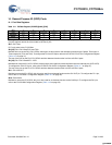
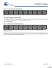
Table 14-4. P3 Data Register (P3DATA) [0x03] [R/W]
Bit # 7 6 5 4 3 2 1 0
Field Reserved P3.1–P3.0
Read/Write - - - - - - R/W R/W
Default 0 0 0 0 0 0 0 0
This register contains the data for Port 3. Writing to this register sets the bit values to be output on output enabled pins. Reading
from this register returns the current state of the Port 3 pins.
Bit [7:2]: Reserved Data [7:2]
Bit [1:0]: P3 Data [1:0]
P3.1–P3.0 only exist in the CY7C638(2/3)3.
[+] Feedback [+] Feedback