CY7C63310, CY7C638xx
Document 38-08035 Rev. *K Page 23 of 83
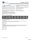
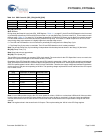
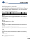
Table 10-4. OSC Control 0 (OSC_CR0) [0x1E0] [R/W]
Bit # 7 6 5 4 3 2 1 0
Field Reserved No Buzz Sleep Timer [1:0] CPU Speed [2:0]
Read/Write – – R/W R/W R/W R/W R/W R/W
Default 0 0 0 0 0 0 0 0
Bit [7:6]: Reserved
Bit 5: No Buzz
During sleep (the Sleep bit is set in the CPU_SCR Register—Table 11-1 on page 27), the LVD and POR detection circuit is turned
on periodically to detect any POR and LVD events on the V
CC
pin (the Sleep Duty Cycle bits in the ECO_TR are used to control
the duty cycle—Table 13-3 on page 32). To facilitate the detection of POR and LVD events, the No Buzz bit is used to force the
LVD and POR detection circuit to be continuously enabled during sleep. This results in a faster response to an LVD or POR
event during sleep at the expense of a slightly higher than average sleep current.
0 = The LVD and POR detection circuit is turned on periodically as configured in the Sleep Duty Cycle.
1 = The Sleep Duty Cycle value is overridden. The LVD and POR detection circuit is always enabled.
Note The periodic Sleep Duty Cycle enabling is independent with the sleep interval shown in the Sleep [1:0] bits below.
Bit [4:3]: Sleep Timer [1:0]
Note Sleep intervals are approximate.
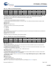
Bit [2:0]: CPU Speed [2:0]
The enCoRe II may operate over a range of CPU clock speeds. The reset value for the CPU Speed bits is zero; as a result, the
default CPU speed is one-eighth of the internal 24 MHz, or 3 MHz
Regardless of the CPU Speed bit’s setting, if the actual CPU speed is greater than 12 MHz, the 24 MHz operating requirements
apply. An example of this scenario is a device that is configured to use an external clock, which supplies a frequency of 20 MHz.
If the CPU speed register’s value is 0b011, the CPU clock is at 20 MHz. Therefore, the supply voltage requirements for the device
are the same as if the part were operating at 24 MHz. The operating voltage requirements are not relaxed until the CPU speed
is at 12 MHz or less.
Note Correct USB operations require the CPU clock speed be at least 1.5 MHz or not less than USB clock/8. If the two clocks
have the same source, then the CPU clock divider must not be set to divide by more than 8. If the two clocks have different
sources, the maximum ratio of USB Clock/CPU Clock must never exceed 8 across the full specification range of both clock
sources.
Note This register exists in the second bank of IO space. This requires setting the XIO bit in the CPU flags register.
CPU Speed
[2:0]
CPU when Internal
Oscillator is selected External Clock
000 3 MHz (Default) Clock In/8
001 6 MHz Clock In/4
010 12 MHz Clock In/2
011 24 MHz Clock In/1
100 1.5 MHz Clock In/16
101 750 kHz Clock In/32
110 187 kHz Clock In/128
111 Reserved Reserved
[+] Feedback [+] Feedback


