CY7C63310, CY7C638xx
Document 38-08035 Rev. *K Page 13 of 83
9. Memory Organization
9.1 Flash Program Memory Organization
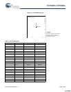
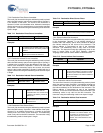
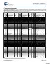
Figure 9-1. Program Memory Space with Interrupt Vector Table
after reset Address
16-bit PC 0x0000 Program execution begins here after a reset
0x0004 POR/LVD
0x0008 INT0
0x000C SPI Transmitter Empty
0x0010 SPI Receiver Full
0x0014 GPIO Port 0
0x0018 GPIO Port 1
0x001C INT1
0x0020 EP0
0x0024 EP1
0x0028 EP2
0x002C USB Reset
0x0030 USB Active
0x0034 1 ms Interval timer
0x0038 Programmable Interval Timer
0x003C Timer Capture 0
0x0040 Timer Capture 1
0x0044 16-bit Free Running Timer Wrap
0x0048 INT2
0x004C PS2 Data Low
0x0050 GPIO Port 2
0x0054 GPIO Port 3
0x0058 Reserved
0x005C Reserved
0x0060 Reserved
0x0064 Sleep Timer
0x0068 Program Memory begins here (if below interrupts not used,
program memory can start lower)
0x0BFF 3 KB ends here (CY7C63310)
0x0FFF 4 KB ends here (CY7C63801)
0x1FFF 8 KB ends here (CY7C638x3)
[+] Feedback [+] Feedback


