CY7C63310, CY7C638xx
Document 38-08035 Rev. *K Page 29 of 83
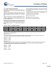
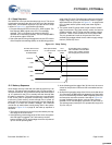
12.1 Sleep Sequence
The SLEEP bit is an input into the sleep logic circuit. This circuit
is designed to sequence the device into and out of the hardware
sleep state. The hardware sequence to put the device to sleep
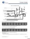
is shown in Figure 12-1. and is defined as follows.
1. Firmware sets the SLEEP bit in the CPU_SCR0 register. The
Bus Request (BRQ) signal to the CPU is immediately
asserted. This is a request by the system to halt CPU
operation at an instruction boundary. The CPU samples BRQ
on the positive edge of CPUCLK.
2. Due to the specific timing of the register write, the CPU issues
a Bus Request Acknowledge (BRA) on the following positive
edge of the CPU clock. The sleep logic waits for the following
negative edge of the CPU clock and then asserts a system
wide Power Down (PD) signal. In Figure 12-1. on page 29 the
CPU is halted and the system wide power down signal is
asserted.
3. The system wide PD (power down) signal controls several
major circuit blocks: The Flash memory module, the internal
24 MHz oscillator, the EFTB filter and the bandgap voltage
reference. These circuits transition into a zero power state.
The only operational circuits on chip are the Low Power
oscillator, the bandgap refresh circuit, and the supply voltage.
monitor. (POR/LVD) circuit.
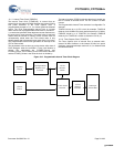
Figure 12-1. Sleep Timing
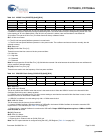
12.2 Wake up Sequence
Once asleep, the only event that can wake the system up is an
interrupt. The global interrupt enable of the CPU flag register is
not required to be set. Any unmasked interrupt wakes the system
up. It is optional for the CPU to actually take the interrupt after
the wake up sequence. The wake up sequence is synchronized
to the 32 kHz clock for purposes of sequencing a startup delay,
to allow the Flash memory module enough time to power up
before the CPU asserts the first read access. Another reason for
the delay is to allow the oscillator, Bandgap, and LVD/POR
circuits time to settle before actually being used in the system.
As shown in Figure 12-2. on page 30, the wake up sequence is
as follows:
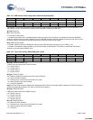
1. The wake up interrupt occurs and is synchronized by the neg-
ative edge of the 32 kHz clock.
2. At the following positive edge of the 32 kHz clock, the system
wide PD signal is negated. The Flash memory module,
internal oscillator, EFTB, and bandgap circuit are all powered
up to a normal operating state.
3. At the following positive edge of the 32 kHz clock, the current
values for the precision POR and LVD have settled and are
sampled.
4. At the following negative edge of the 32 kHz clock (after about
15 µS nominal), the BRQ signal is negated by the sleep logic
circuit. On the following CPUCLK, BRA is negated by the CPU
and instruction execution resumes. Note that in Figure 12-2.
on page 30 fixed function blocks, such as Flash, internal
oscillator, EFTB, and bandgap, have about 15 µSec start up.
The wakeup times (interrupt to CPU operational) range from
75 µS to 105 µS.
Firmware write to SCR
SLEEP bit causes an
immediate BRQ
IOW
SLEEP
BRQ
PD
BRA
CPUCLK
CPU captures BRQ
on next CPUCLK
edge
CPU
responds with
a BRA
On the falling edge of CPUCLK,
PD is asserted. The 24/48 MHz
system clock is halted; the Flash
and bandgap are powered down
[+] Feedback [+] Feedback


