CY7C63310, CY7C638xx
Document 38-08035 Rev. *K Page 57 of 83
19. USB/PS2 Transceiver
Although the USB transceiver has features to assist in interfacing to PS/2, these features are not controlled using these registers. The
registers only control the USB interfacing features. PS/2 interfacing options are controlled by the D+ and D– GPIO Configuration
register (See Table 14-2 on page 34).
19.1 USB Transceiver Configuration
20. USB Serial Interface Engine (SIE)
The SIE allows the microcontroller to communicate with the USB
host at low speed data rates (1.5 Mbps). The SIE simplifies the
interface between the microcontroller and the USB by incorpo-
rating hardware that handles the following USB bus activity
independently of the microcontroller.
■
Translate the encoded received data and format the data to be
transmitted on the bus.
■
CRC checking and generation. Flag the microcontroller if errors
exist during transmission.
■
Address checking. Ignore the transactions not addressed to
the device.
■
Send appropriate ACK/NAK/STALL handshakes.
■
Token type identification (SETUP, IN, or OUT). Set the
appropriate token bit after a valid token is received.
■
Place valid received data in the appropriate endpoint FIFOs.
■
Send and update the data toggle bit (Data1/0).
■
Bit stuffing and unstuffing.
Firmware is required to handle the rest of the USB interface with
the following tasks:
■
Coordinate enumeration by decoding USB device requests.
■
Fill and empty the FIFOs.
■
Suspend and Resume coordination.
■
Verify and select Data toggle values.
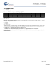
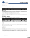
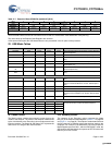
Table 19-1. USB Transceiver Configure Register (USBXCR) [0x74] [R/W]
Bit # 7 6 5 4 3 2 1 0
Field USB Pull up
Enable
Reserved USB Force State
Read/Write R/W – – – – – – R/W
Default 0 0 0 0 000 0
Bit 7: USB Pull up Enable
0 = Disable the pull up resistor on D–
1 = Enable the pull up resistor on D–. This pull up is to V
CC
if the PHY’s internal voltage regulator is not enabled or to the internally
generated 3.3V when VREG is enabled.
Bit [6:1]: Reserved
Bit 0: USB Force State
This bit allows the state of the USB IO pins D– and D+ to be forced to a state when USB is enabled.
0 = Disable USB Force State
1 = Enable USB Force State. Allows the D– and D+ pins to be controlled by P1.1 and P1.0 respectively when the USBIO is in
USB mode. Refer to Table 14-2 on page 34 for more information.
Note The USB transceiver has a dedicated 3.3V regulator for USB signalling purposes and to provide for the 1.5K D– pull up.
Unlike the other 3.3V regulator, this regulator cannot be controlled or accessed by firmware. When the device is suspended,
this regulator is disabled along with the bandgap (which provides the reference voltage to the regulator) and the D– line is
pulled up to 5V through an alternate 6.5K resistor. During wake up following a suspend, the band gap and the regulator are
switched on in any order. Under an extremely rare case when the device wakes up following a bus reset condition and the volt-
age regulator and the band gap turn on in that particular order, there is possibility of a glitch or low pulse occurring on the D–
line. The host can misinterpret this as a deattach condition. This condition, although rare, is avoided by keeping the bandgap
circuitry enabled during sleep. This is achieved by setting the ‘No Buzz’ bit, bit[5] in the OSC_CR0 register. This is an issue
only if the device is put to sleep during a bus reset condition.
[+] Feedback [+] Feedback


