CY7C63310, CY7C638xx
Document 38-08035 Rev. *K Page 8 of 83
7. CPU Registers
The CPU registers in enCoRe II devices are in two banks with 256 registers in each bank. Bit[4]/XIO bit in the CPU Flags register
must be set/cleared to select between the two register banks Table 7-1 on page 8
7.1 Flags Register
The Flags Register is set or reset only with logical instruction.
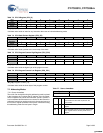
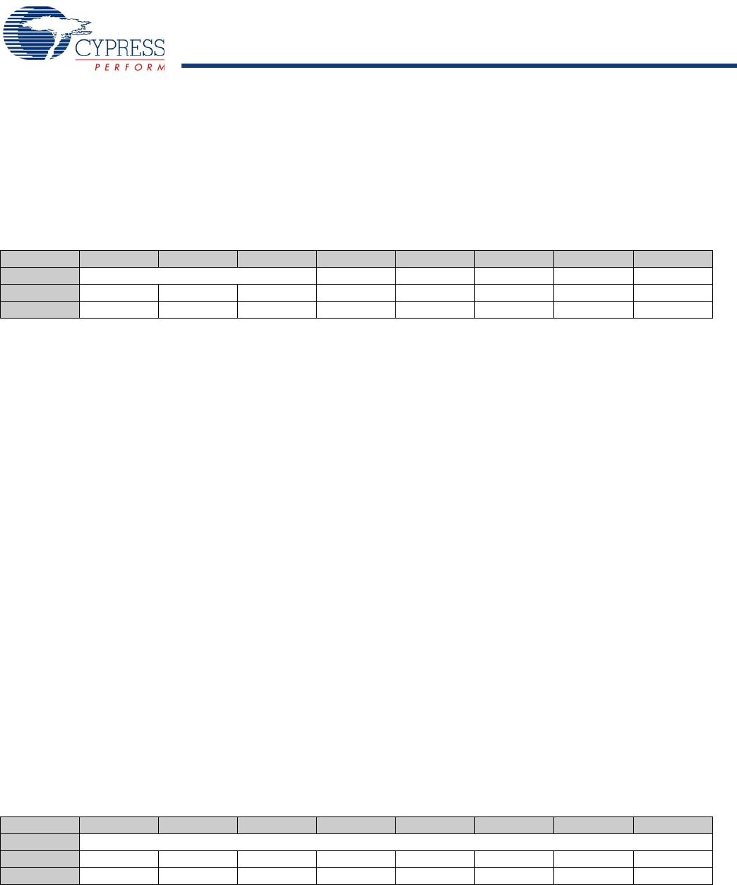
Table 7-1. CPU Flags Register (CPU_F) [R/W]
Bit # 7 6 5 4 3 2 1 0
Field Reserved XIO Super Carry Zero Global IE
Read/Write – – – R/W R RW RW RW
Default 00000010
Bit [7:5]: Reserved
Bit 4: XIO
Set by the user to select between the register banks
0 = Bank 0
1 = Bank 1
Bit 3: Super
Indicates whether the CPU is executing user code or Supervisor Code. (This code cannot be accessed directly by the user.)
0 = User Code
1 = Supervisor Code
Bit 2: Carry
Set by the CPU to indicate whether there has been a carry in the previous logical/arithmetic operation.
0 = No Carry
1 = Carry
Bit 1: Zero
Set by the CPU to indicate whether there has been a zero result in the previous logical/arithmetic operation.
0 = Not Equal to Zero
1 = Equal to Zero
Bit 0: Global IE
Determines whether all interrupts are enabled or disabled
0 = Disabled
1 = Enabled
Note CPU_F register is only readable with the explicit register address 0xF7. The OR F, expr and AND F, expr instructions must
be used to set and clear the CPU_F bits.
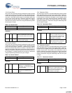
Table 7-2. CPU Accumulator Register (CPU_A)
Bit # 7 6 5 4 3 2 1 0
Field CPU Accumulator [7:0]
Read/Write ––––––––
Default 00000000
Bit [7:0]: CPU Accumulator [7:0]
8-bit data value holds the result of any logical/arithmetic instruction that uses a source addressing mode
[+] Feedback [+] Feedback


