


S1F79100Y Series
3–36 EPSON S1F70000 Series
Technical Manual
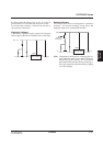
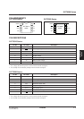
Differential amplifier
The built-in differential amplifier generates a potential
at point X that adjusts the gate bias of the output transis-
tor if there is any difference betweeen V
REF and VREG.
V
REG
To output
transistor
V
SS
V
REF
V
I
N1 N2
P1 P2
X
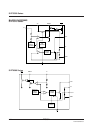
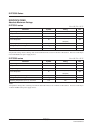
Output transistor
The output side of the p-channel MOS transistors in the
output transistor circuit is connected to the voltage di-
vider resistors in the feedback loop.
R
1
V
REG
V
REF
+
–
V
1
V
O
V
SS
R
2
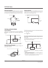
TYPICAL APPLICATIONS
Current Booster
At the cost of a small increase in current consumption,
the voltage is regulated while maintaining high current
output.
GND
V
O
V
I
V
O
V
SS
V
I
S1F79100Y
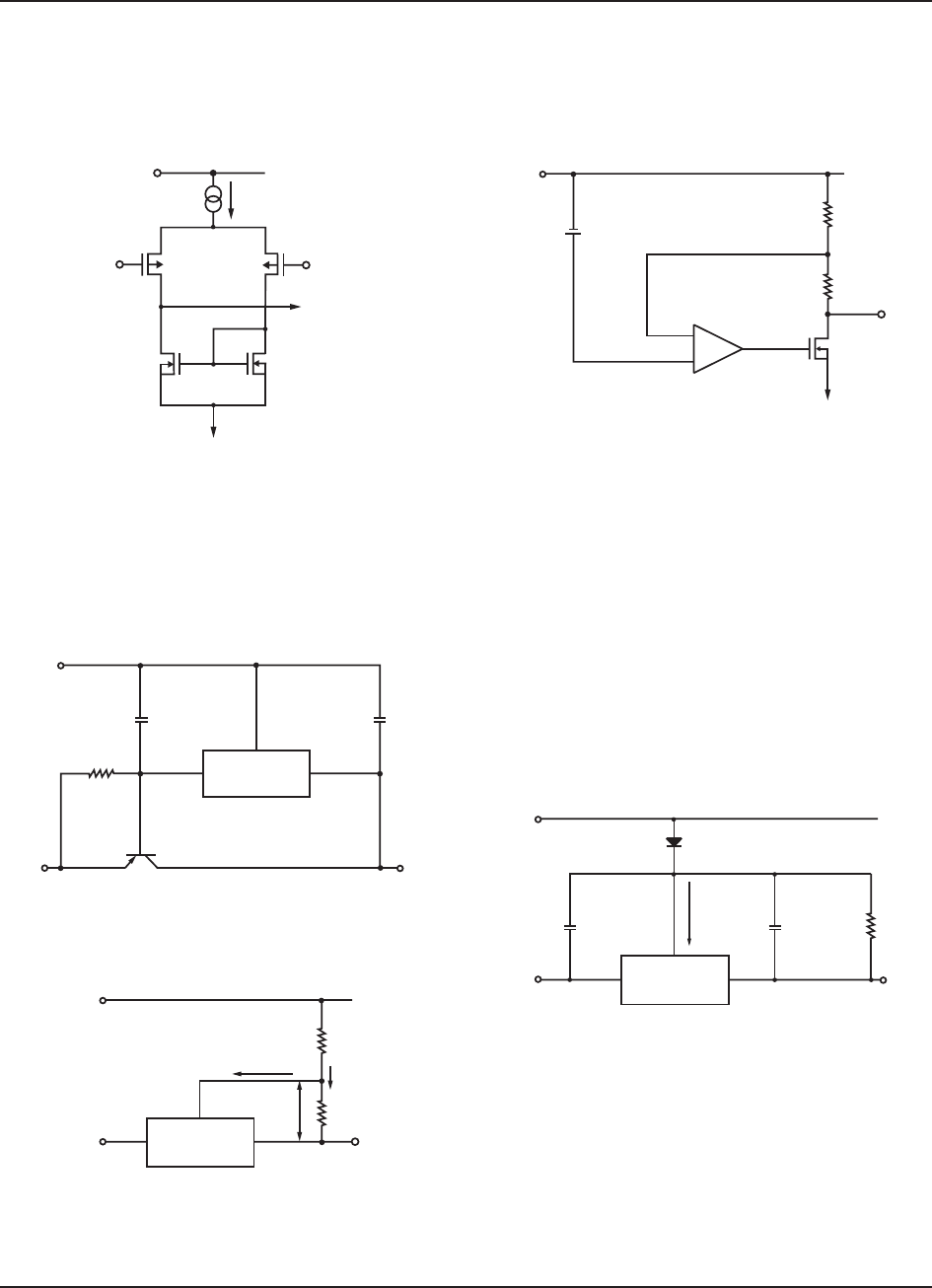
External Voltage Converter
The following circuit raises the output voltage of a
S1F79100Y series IC.
R
1
I
OPR
GND
V
O
V
O
V
r
V
I
V
I
V
SS
R
2
I
B
S1F79100Y
The following equation shows the relationship between
the old and new voltages.
R
1 + R2
VO =—————VR
R2
Note that the application must supply a bias current, IB,
high enough to offset the increase in voltage across R
1
due to IOPR.
An alternative circuit for raising the output voltage is
shown in the following figure.
V
O
V
I
R1C
O
C
I
GND
V
I
I
SS
V
O
V
SS
S1F79100Y
This configuration, however, introduces two design
problems.
1. It reduces the output voltage by V
F, the forward volt-
age drop across the diode.
2. It is sensitive to fluctuations in V
F due to differences
in diodes, operating temperatures and I
SS.